“99.9% alumina” is a common ceramic specification.
For semiconductor equipment, however, this number does not tell the whole story.
Two ceramic components can both contain 99.9% Al₂O₃ and still behave very differently inside a plasma-processing chamber.
The reason is microstructure.
Porosity, grain size, grain-boundary chemistry and sintering history can influence erosion, contamination and particle generation just as strongly as nominal purity.
Why Purity Became the First Screening Parameter
Lower-purity alumina can contain larger amounts of:
- SiO₂;
- CaO;
- MgO;
- alkali compounds;
- glassy secondary phases.
These materials help densification and manufacturing, but some may be less stable than alumina in semiconductor process environments.
As a result, higher-purity alumina is generally preferred for critical chamber components.
But once purity becomes very high, other variables become dominant.
Density and Porosity Matter
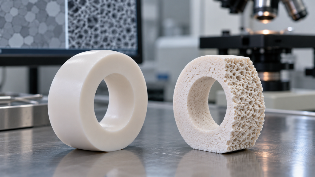
Imagine two 99.9% alumina parts.
One is almost fully dense.
The other contains interconnected pores near the surface.
When plasma reaches those pores, the effective exposed surface area increases.
Localized erosion can occur around pore boundaries.
Eventually, individual grains may become unsupported and detach.
This creates particles.
Therefore, a dense 99.9% alumina ceramic can perform very differently from a porous material with the same chemistry.
2026 Research Highlights Processing
A 2026 study specifically investigated how slurry preparation and sintering atmosphere affect dense plasma-resistant alumina ceramics.
The researchers examined milling, slurry aging and firing conditions and linked these processing steps with densification, mechanical strength and plasma resistance.
The important industrial lesson is simple:
final ceramic performance begins long before the finished component reaches the grinding machine.
Powder and slurry processing determine the microstructure that later becomes the plasma-facing surface.
Why Slurry Processing Matters
Ceramic powder needs to be dispersed uniformly.
Poor dispersion can create:
- agglomerates;
- local density variation;
- pores;
- abnormal grain growth.
These defects may remain after sintering.
A polished surface can hide some microstructural problems visually, but plasma exposure may reveal them later through localized erosion.
This means manufacturing consistency depends on controlled powder preparation, mixing and forming.
Sintering Controls Grain Boundaries
During sintering, ceramic particles bond and densify.
Temperature and atmosphere influence:
- final density;
- grain growth;
- residual pores;
- secondary phases;
- mechanical strength.
For semiconductor ceramics, the ideal microstructure is not simply “large grains” or “small grains.”
The objective is a dense, homogeneous microstructure that remains stable under the intended plasma chemistry.
Surface Finish Cannot Fix Internal Porosity
Precision grinding and polishing can create an extremely smooth surface.
However, polishing cannot change the bulk microstructure.
If the ceramic contains subsurface pores or weak grain boundaries, plasma exposure may gradually uncover them.
This is why surface roughness and bulk density should be evaluated separately.
A component can have excellent Ra and still show poor plasma durability.
Semiconductor-Grade Should Mean More Than Purity
A more complete RFQ for a semiconductor alumina part may include:
- nominal Al₂O₃ purity;
- density;
- open porosity;
- individual metallic impurities;
- grain-size range;
- surface roughness;
- dimensional tolerances;
- cleaning procedure;
- packaging requirements.
For plasma-facing parts, a process-specific erosion test may also be necessary.
Plasma Resistance Is Process-Specific
Alumina can perform well in many semiconductor environments, but no single erosion number applies to every etch chamber.
Performance changes with:
- fluorine concentration;
- ion energy;
- RF bias;
- temperature;
- plasma density;
- exposure time.
Recent research into plasma-resistant coatings has reinforced the broader point that corrosion rate and particle generation must be considered together.
Why This Matters for Replacement Parts
Replacement ceramic parts are sometimes sourced by matching:
material + drawing dimensions.
For semiconductor equipment, that can be insufficient.
A replacement part with the same dimensions and nominal purity may show:
- different chamber seasoning;
- different particle behavior;
- different lifetime.
The manufacturing history of the ceramic can therefore influence process stability.
Päätelmä
Purity remains important.
But the industry is moving beyond a simple “95% vs 99.5% vs 99.9%” comparison.
For advanced semiconductor equipment, a better question is:
What microstructure does that purity produce?
The highest-value ceramic is not necessarily the one with the largest purity number.
It is the material that consistently delivers:
high density + stable grain boundaries + controlled impurities + low particle generation.