
As emerging technologies such as electric vehicles (EVs), 5G communications, renewable energy systems, artificial intelligence (AI), aerospace electronics, and power semiconductors continue to evolve, electronic devices are becoming increasingly powerful, compact, and highly integrated. While these advancements improve performance, they also generate significantly higher heat densities, creating critical challenges for thermal management and device reliability.
Efficient heat dissipation has become one of the most important factors determining the lifespan, performance, and safety of modern electronic systems. Among various packaging and thermal management materials, ceramic substrates have emerged as indispensable components due to their unique combination of high thermal conductivity, excellent electrical insulation, mechanical strength, and chemical stability.
Heute, Keramiksubstrate serve as the foundation of numerous high-power electronic and optoelectronic devices, playing a crucial role in power modules, LED packaging, RF components, laser systems, and semiconductor packaging technologies.
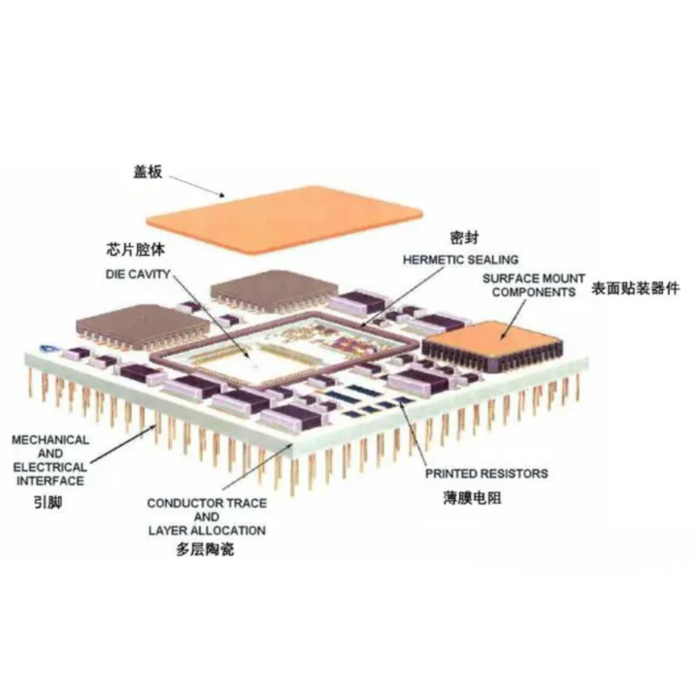
What Is a Ceramic Substrate?
A ceramic substrate is a specialized electronic packaging material that provides mechanical support, electrical interconnection, insulation, and thermal dissipation for semiconductor devices.
Unlike conventional organic circuit boards, ceramic substrates are designed to withstand extreme temperatures, high voltages, and demanding operating environments while efficiently transferring heat away from sensitive semiconductor chips.
In modern electronic packaging systems, ceramic substrates function as:
- Structural support for semiconductor devices
- Electrical insulation between conductive layers
- Heat spreaders for thermal management
- Interconnection platforms for integrated circuits
- Protective barriers against environmental degradation
As power densities continue to increase, ceramic substrates are becoming essential for maintaining device efficiency and long-term reliability.
Why Ceramic Substrates Are Important
Electronic devices generate heat during operation. If this heat is not removed efficiently, several problems may occur:
- Reduced device efficiency
- Accelerated material degradation
- Increased failure rates
- Thermal runaway in power electronics
- Reduced operational lifetime
Ceramic materials offer several advantages over traditional organic substrates:
Hohe Wärmeleitfähigkeit
Efficient heat transfer helps maintain lower junction temperatures and improves device reliability.
Hervorragende elektrische Isolierung
Ceramics combine electrical insulation with thermal conductivity, a rare and highly valuable combination for power electronics.
Thermal Expansion Compatibility
Many ceramic materials exhibit thermal expansion coefficients closer to semiconductor materials, reducing thermal stress during operation.
Chemical and Environmental Stability
Ceramic substrates maintain stable performance under corrosive gases, humidity, radiation exposure, and high temperatures.
Mechanische Festigkeit
Advanced ceramics provide excellent rigidity and wear resistance, ensuring long-term structural integrity.
Major Ceramic Substrate Materials
Tonerde (Al₂O₃)
Alumina remains the most widely used ceramic substrate material worldwide.
Vorteile
- Low material cost
- Mature manufacturing technology
- Hervorragende elektrische Isolierung
- Good mechanical properties
- High chemical resistance
Limitations
Its thermal conductivity is relatively low, typically around 20–35 W/m·K.
Anwendungen
- Kfz-Elektronik
- LED lighting
- Consumer electronics
- Industrial control systems
Because of its cost-effectiveness, alumina accounts for the majority of ceramic substrate production globally.
Aluminiumnitrid (AlN)
Aluminum nitride has become one of the most important materials for high-performance electronic packaging.
Wesentliche Merkmale
- Thermal conductivity exceeding 170 W/m·K
- Niedrige Dielektrizitätskonstante
- Excellent insulation properties
- Wärmeausdehnungskoeffizient nahe dem von Silizium
Anwendungen
- Leistungshalbleitermodule
- Laser diode packaging
- RF-Geräte
- High-power LEDs
- Data center electronics
Its superior thermal performance makes AlN a preferred choice for advanced thermal management applications.
Siliziumnitrid (Si₃N₄)
Silicon nitride is widely recognized for its exceptional mechanical performance.
Vorteile
- Hohe Bruchzähigkeit
- Ausgezeichnete Temperaturwechselbeständigkeit
- High flexural strength
- Superior reliability under cyclic loading
Anwendungen
- Electric vehicle power modules
- Railway traction systems
- Wind power converters
- Aerospace electronics
As silicon carbide (SiC) power devices become more prevalent, silicon nitride substrates are increasingly favored due to their outstanding reliability.
Beryllium Oxide (BeO)
Beryllium oxide exhibits extremely high thermal conductivity, often exceeding 250 W/m·K.
Vorteile
- Ausgezeichnete Wärmeleitfähigkeit
- Geringer dielektrischer Verlust
- High-frequency performance
Limitations
The toxicity of beryllium-containing materials requires strict handling and manufacturing controls.
As a result, BeO is generally limited to specialized aerospace, defense, and high-frequency applications.
Ceramic Substrate Manufacturing Technologies
Different metallization and fabrication processes produce ceramic substrates with distinct performance characteristics.
Direct Bonded Copper (DBC)
DBC technology bonds copper foil directly onto ceramic surfaces through high-temperature processing.
Vorteile
- Thick copper layers
- High current carrying capability
- Ausgezeichnete Wärmeleitfähigkeit
Gängige keramische Materialien
- Tonerde
- Aluminum nitride
Typische Anwendungen
- IGBT-Module
- EV inverters
- Erneuerbare Energiesysteme
- Industrial motor drives
DBC remains one of the most widely used technologies in power electronics.
Active Metal Brazing (AMB)
AMB technology employs active brazing alloys containing reactive elements such as titanium to achieve strong bonding between metals and ceramics.
Vorteile
- Higher bonding strength
- Improved thermal cycling reliability
- Better mechanical robustness
Anwendungen
- Silicon carbide power modules
- Electric vehicle traction systems
- High-voltage power conversion
- Railway transportation
AMB has become increasingly important for next-generation wide-bandgap semiconductor packaging.
Direct Plated Copper (DPC)
DPC utilizes thin-film deposition and electroplating technologies to form highly precise conductive circuits on ceramic surfaces.
Vorteile
- Fine line resolution
- Excellent dimensional accuracy
- Suitable for miniaturized packaging
Anwendungen
- High-power LEDs
- Optical communication devices
- Laser packaging
- Sensors
The technology is particularly attractive for optoelectronic and photonic applications.
High-Temperature Co-Fired Ceramics (HTCC)
HTCC technology involves co-firing ceramic layers and refractory metal conductors at temperatures exceeding 1,500°C.
Anwendungen
- Aerospace electronics
- Military electronics
- Hochtemperatursensoren
HTCC offers excellent reliability under harsh operating conditions.
Low-Temperature Co-Fired Ceramics (LTCC)
LTCC technology reduces firing temperatures to approximately 850°C, enabling the use of highly conductive metals such as silver and copper.
Vorteile
- Three-dimensional circuit integration
- Excellent RF performance
- Compact package design
Anwendungen
- 5G communication systems
- Microwave devices
- Radar systems
- IoT modules
LTCC is considered a key enabling technology for high-frequency electronic systems.
Ceramic Substrates in Power Electronics
Power semiconductor devices generate substantial heat during operation.
Modern power modules based on:
- Silicon (Si)
- Siliziumkarbid (SiC)
- Gallium Nitride (GaN)
require substrate materials capable of handling:
- Hohe Temperaturen
- High voltages
- Large current densities
Ceramic substrates provide the necessary combination of thermal conductivity and electrical insulation, making them fundamental components in power conversion systems.
Die Anwendungen umfassen:
- Elektrische Fahrzeuge
- Fast charging stations
- Solar inverters
- Wind energy systems
- Industrial automation
Ceramic Substrates in Optoelectronics
Beyond power electronics, ceramic substrates are increasingly used in optoelectronic applications.
Beispiele hierfür sind:
LED Packaging
Ceramic substrates improve heat dissipation and light output efficiency.
Laser Diodes
High thermal conductivity minimizes thermal distortion and wavelength drift.
Optical Communication Devices
Precise thermal control enhances signal stability and transmission performance.
Photonic Integrated Circuits
Advanced ceramic packaging solutions support higher integration densities and improved reliability.
Zukünftige Trends
Wide-Bandgap Semiconductor Packaging
The rapid adoption of SiC and GaN devices will drive demand for high-performance ceramic substrates.
High-Thermal-Conductivity Materials
Researchers continue developing ceramic materials with thermal conductivities exceeding current commercial standards.
Advanced Multilayer Packaging
Future ceramic substrates will integrate thermal management, electrical interconnection, and sensing functions into a single platform.
AI and Data Center Applications
Growing computing power requirements are creating new opportunities for ceramic thermal management solutions.
Aerospace and Space Electronics
Extreme-environment electronics will increasingly rely on advanced ceramic packaging technologies.
Schlussfolgerung
Ceramic substrates have become one of the most critical enabling materials in modern electronics. Their unique ability to combine thermal conductivity, electrical insulation, mechanical strength, and environmental stability makes them indispensable in power electronics, optoelectronics, telecommunications, renewable energy systems, and aerospace applications.
As the semiconductor industry transitions toward higher power densities and next-generation wide-bandgap devices, ceramic substrate technologies such as DBC, AMB, DPC, LTCC, and HTCC will continue to play a pivotal role. Ongoing advances in ceramic materials and manufacturing processes are expected to further improve performance, reliability, and integration, supporting the future development of high-efficiency electronic and photonic systems worldwide.

