產業新聞

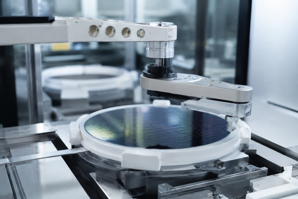
半導體設備中的先進陶瓷材料:應用與材料比較

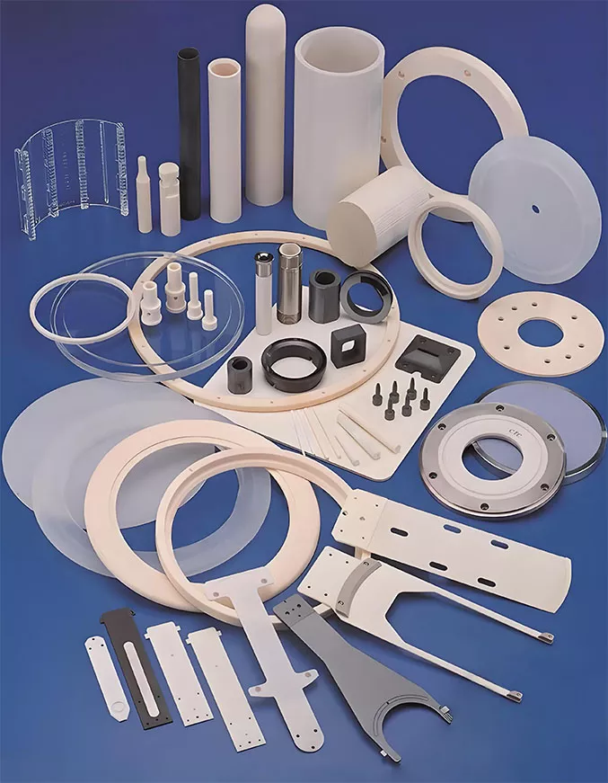
In modern semiconductor manufacturing equipment, advanced ceramics are no longer optional components—they are critical enabling materials that determine precision, stability, and process reliability. From plasma etching chambers to wafer handling systems, different ceramic materials are selected based on thermal, electrical, and mechanical performance requirements. This article introduces the most widely used semiconductor-grade ceramics and provides […]
半導體設備中的先進陶瓷材料:應用與材料比較 閱讀更多 »

高性能熱管理:氧化鋁陶瓷散熱器取代傳統金屬解決方案的原因

As electronic devices continue to evolve toward higher power density, efficient heat dissipation has become one of the most critical challenges in modern engineering. Traditional metal heat sinks such as aluminum and copper are no longer sufficient in applications requiring both electrical insulation and thermal stability. This is where the alumina ceramic heat sink (Al₂O₃)

高性能熱管理:氧化鋁陶瓷散熱器取代傳統金屬解決方案的原因 閱讀更多 »

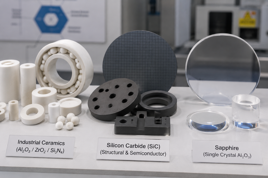
工業陶瓷 vs 碳化矽 vs 藍寶石:結構與功能材料的觀點

In advanced engineering industries such as semiconductors, precision machinery, and optical systems, industrial ceramics, silicon carbide (SiC), and sapphire are often compared as competing materials. However, this comparison is misleading if treated as a simple “which is better” question. A more accurate understanding is: These three materials represent three different material architectures, not just three

工業陶瓷 vs 碳化矽 vs 藍寶石:結構與功能材料的觀點 閱讀更多 »

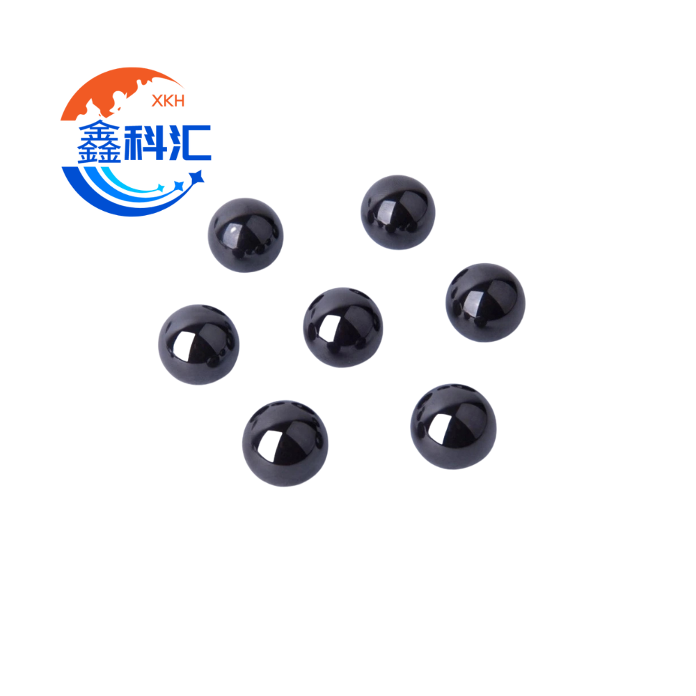
軸承用精密陶瓷球:材料選擇與性能

Precision ceramic balls are widely used in modern high-performance bearings where speed, reliability, and service life are critical. Compared with traditional steel balls, ceramic materials offer distinct advantages in friction reduction, wear resistance, and high-speed operation, making them essential components in aerospace, electric vehicles, precision machinery, and advanced manufacturing equipment. This article explains the main

軸承用精密陶瓷球:材料選擇與性能 閱讀更多 »

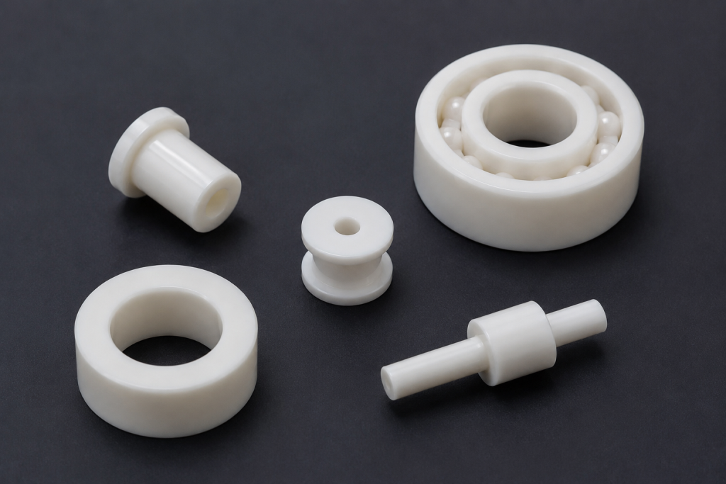
氧化鋯陶瓷零件如何提高設備壽命

Modern industrial equipment operates under increasingly demanding conditions. Higher speeds, elevated temperatures, abrasive environments, and continuous operation place tremendous stress on machine components. As industries pursue greater efficiency and lower maintenance costs, material selection has become a critical factor affecting system reliability and service life. Among advanced engineering ceramics, zirconia ceramic (ZrO₂) has gained significant

氧化鋯陶瓷零件如何提高設備壽命 閱讀更多 »

氧化鋯與氧化鋁:哪種陶瓷材料性能更好?

Advanced ceramics have become essential materials in industries requiring exceptional wear resistance, high strength, thermal stability, and chemical durability. Among the most widely used engineering ceramics, zirconia (ZrO₂) and alumina (Al₂O₃) stand out due to their broad industrial applications and excellent performance characteristics. However, engineers and purchasing teams often face a key question: Which ceramic

氧化鋯與氧化鋁:哪種陶瓷材料性能更好? 閱讀更多 »

用於半導體製造的結構陶瓷:材料、應用與未來趨勢

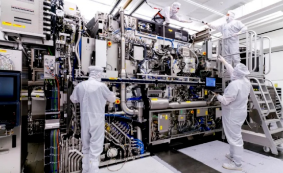
Modern semiconductor manufacturing requires unprecedented levels of precision, cleanliness, thermal stability, and reliability. As chip architectures continue to evolve toward smaller nodes, higher power density, and advanced packaging technologies, conventional metallic materials increasingly face limitations in process environments involving plasma exposure, ultra-high vacuum, aggressive chemicals, and extreme temperatures. Structural ceramics have therefore become indispensable materials

用於半導體製造的結構陶瓷:材料、應用與未來趨勢 閱讀更多 »

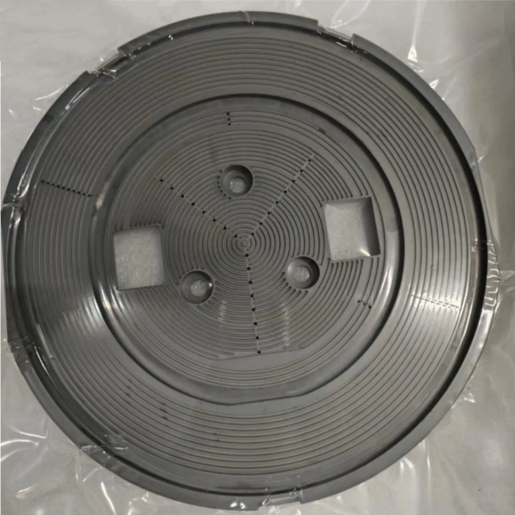
陶瓷真空吸盤

多孔陶瓷在半導體製造中的應用:透過先進材料設計實現精準度

Porous ceramics are engineered ceramic materials produced through specialized processing techniques that create interconnected or closed pore structures within the material. Their porosity typically ranges from 20% to 90%, while pore sizes can vary from nanometer scale to millimeter scale depending on design requirements. Thanks to their unique internal architecture and outstanding physical properties—including high-temperature

多孔陶瓷在半導體製造中的應用:透過先進材料設計實現精準度 閱讀更多 »

半導體陶瓷解析:改變現代科技的功能性電子陶瓷

Semiconductor ceramics are a specialized class of electronic ceramic materials engineered to exhibit semiconductor behavior through controlled material modification. Unlike traditional conductive materials, their electrical properties are highly sensitive to external conditions such as temperature, light, electric fields, humidity, and surrounding gases. This unique responsiveness allows semiconductor ceramics to convert environmental changes into electrical signals,

半導體陶瓷解析:改變現代科技的功能性電子陶瓷 閱讀更多 »

陶瓷基板:推動人工智慧運算、光學模組和功率半導體的核心材料革命

As artificial intelligence computing accelerates, data transmission speeds increase, and next-generation power electronics continue to evolve, semiconductor packaging technologies are undergoing a fundamental transformation. Conventional substrate materials are increasingly facing limitations in thermal management, electrical performance, and integration density. Against this backdrop, ceramic substrates are emerging from niche applications to become critical enabling materials for

陶瓷基板:推動人工智慧運算、光學模組和功率半導體的核心材料革命 閱讀更多 »

半導體設備中的氧化鋁陶瓷元件:功能、結構和先進應用

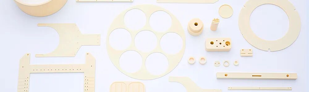
As semiconductor devices continue evolving toward smaller nodes, higher integration density, and greater processing precision, the demand for ultra-clean, heat-resistant, and plasma-stable materials inside semiconductor equipment has increased significantly. Among advanced engineering ceramics, high-purity alumina ceramic (Al₂O₃) remains one of the most widely used materials across semiconductor manufacturing systems. From plasma etching chambers to wafer

半導體設備中的氧化鋁陶瓷元件:功能、結構和先進應用 閱讀更多 »

半導體設備的精密陶瓷元件:先進陶瓷應用的全面概述

As semiconductor manufacturing advances toward smaller process nodes, higher integration density, and ultra-clean production environments, precision ceramic components have become indispensable throughout semiconductor fabrication equipment. Advanced ceramics are widely used in lithography, etching, thin-film deposition, ion implantation, CMP, packaging, and wafer handling systems. These ceramic components serve critical functions including wafer support, plasma resistance, insulation,

半導體設備的精密陶瓷元件:先進陶瓷應用的全面概述 閱讀更多 »