
Modern semiconductor manufacturing relies heavily on advanced equipment such as etching systems, lithography machines, ion implantation tools, and deposition equipment. Inside these systems, numerous ceramic components play critical roles in ensuring process stability, precision, and reliability.
Thanks to their exceptional high-temperature resistance, corrosion resistance, mechanical strength, dimensional stability, and electrical properties, advanced ceramic components are widely used throughout semiconductor fabrication processes. Many of these components come into direct contact with wafers and are responsible for precise temperature control, plasma resistance, vacuum handling, and contamination reduction.
Common semiconductor ceramic materials include:
- 氧化鋁 (Al₂O₃)
- 碳化矽 (SiC)
- 氮化鋁 (AlN)
- 氮化矽 (Si₃N₄)
- 釓賴 (Y₂O₃)
Typical 半導體陶瓷元件 include:
- Ceramic robot arms (end effectors)
- Ceramic nozzles
- Ceramic windows
- Chamber liners and shields
- Porous ceramic vacuum chucks
- 靜電夾頭
- 晶圓處理元件
The manufacturing of semiconductor ceramic parts involves a series of highly controlled processes, including powder preparation, forming, sintering, precision machining, inspection, and surface treatment.
1. Powder Preparation
The quality of ceramic components begins with the preparation of high-purity ceramic powders.
Raw Material Formulation
The first step is selecting and mixing ultra-fine ceramic raw materials according to a specific formulation.
Depending on the material requirements, ceramic powders can be synthesized using:
- Solid-state methods
- Liquid-phase methods
- Gas-phase methods
The objective is to achieve high purity, controlled particle size distribution, and excellent chemical uniformity.
Ball Milling
Ball milling is commonly used to refine ceramic powders and improve particle uniformity.
During this process:
- Ceramic powders are loaded into a ball mill.
- Ceramic or polymer-lined milling chambers are used to minimize contamination.
- Grinding media, typically ceramic balls, are added.
Through continuous impact and friction, powder particles are reduced to micron or even submicron sizes, improving sintering performance and final material density.
Spray Drying
After powder synthesis, ceramic slurries often require washing, filtration, drying, and calcination. These processes can affect particle morphology and compositional consistency.
Spray drying offers a more controlled solution.
In this process:
- The ceramic slurry is atomized into fine droplets.
- The droplets are introduced into a stream of hot air.
- Solvent rapidly evaporates.
- Uniform spherical granules are formed.
Benefits of spray drying include:
- Consistent particle size distribution
- Improved powder flowability
- Better mold filling during forming
- Finer grain structures after sintering
2. Ceramic Forming Processes
After powder preparation, ceramic powders are shaped into “green bodies” before sintering.
Several forming technologies are commonly used depending on the geometry and performance requirements of the final component.
乾壓
Dry pressing is one of the most widely used ceramic forming methods.
Process
- Granulated powder is filled into a precision metal mold.
- Pressure is applied through punches.
- Powder particles compact under load.
- A green body with sufficient strength and shape is produced.
優勢
- High production efficiency
- Excellent dimensional consistency
- Suitable for simple geometries
- Cost-effective for mass production
應用
- 陶瓷基板
- Discs
- Rings
- Structural ceramic components
等靜壓
Isostatic pressing provides uniform compaction from all directions.
Process
The ceramic powder compact is placed inside a flexible mold and loaded into an isostatic press.
A liquid pressure medium is used to apply pressure uniformly throughout the component.
Since pressure is transmitted equally in every direction:
- Density distribution becomes more uniform.
- Internal stress is reduced.
- Mechanical properties are improved.
優勢
- Higher green density
- Improved structural integrity
- Reduced deformation during sintering
- Suitable for large or complex parts
應用
- Semiconductor ceramic chambers
- Large SiC components
- High-performance structural ceramics
Tape Casting
Tape casting is a specialized forming technology used for producing thin ceramic sheets.
Process
A well-dispersed ceramic slurry is continuously cast onto a carrier film through a doctor blade.
The slurry spreads evenly and forms a thin layer.
After drying:
- Solvent evaporates.
- Organic binders create a flexible network.
- Thin ceramic tapes are produced.
The tapes can then undergo:
- 切割
- Punching
- Hole formation
- Lamination
before being fired.
優勢
- Thickness control from tens of microns to several millimeters
- Excellent surface flatness
- 高尺寸精度
應用
- 陶瓷基板
- 電子封裝
- Multilayer ceramic devices
- Sensor components
Ceramic Injection Molding (CIM)
Ceramic Injection Molding combines ceramic powders with polymer binders to form complex shapes.
Process
- Ceramic powder is mixed with thermoplastic binders.
- The feedstock is heated into a flowable state.
- Material is injected into a mold cavity.
- The molded part cools and solidifies.
- The green body is ejected.
Subsequent debinding and sintering produce the final ceramic component.
優勢
- Excellent for complex geometries
- High production efficiency
- 嚴格的尺寸公差
- Automated manufacturing capability
應用
- Semiconductor nozzles
- Precision ceramic insulators
- 晶圓處理元件
- Miniature ceramic structures
Gel Casting
Gel casting is an advanced near-net-shape forming technology suitable for complex ceramic parts.
Process
A low-viscosity ceramic slurry with high solid loading is prepared.
Organic monomers and initiators are added to the slurry.
After casting into a mold:
- Polymerization occurs in situ.
- A three-dimensional network forms.
- The slurry solidifies into a rigid body.
The green body then undergoes:
- Demolding
- Drying
- Debinding
- Sintering
to produce the final ceramic component.
優勢
- High green strength
- Excellent shape complexity
- Low shrinkage
- Uniform density distribution
應用
- Complex semiconductor ceramic components
- Large precision ceramic structures
- Customized high-performance ceramic parts
Beyond Forming: Sintering, Machining, and Surface Engineering
Although forming is a critical step, semiconductor ceramic components require additional processing before becoming finished products.
高溫燒結
Green bodies are densified through high-temperature sintering, often exceeding:
- 1,600°C for alumina
- 1,800°C for silicon nitride
- 2,000°C or higher for certain silicon carbide materials
This process develops the ceramic’s final microstructure and mechanical properties.
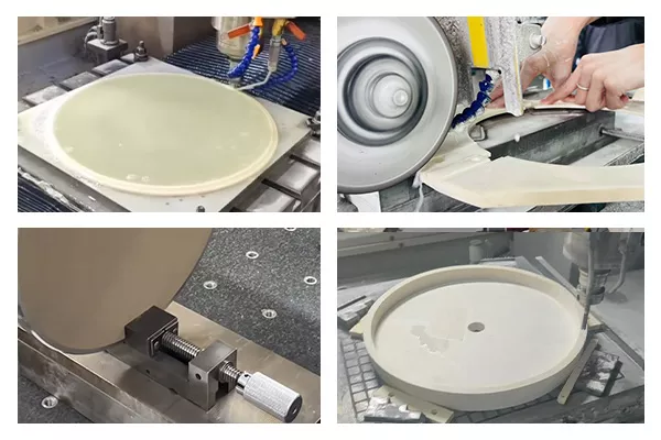
Precision Machining
Because semiconductor equipment demands micron-level accuracy, advanced machining techniques are often required, including:
- 鑽石研磨
- CNC 加工
- Laser machining
- 超音波加工
- Precision polishing
表面處理
Additional treatments may include:
- Plasma-resistant coatings
- Yttria coatings
- 表面拋光
- Cleaning and contamination control processes
These treatments enhance performance and extend service life in harsh semiconductor environments.
總結
The manufacturing of semiconductor ceramic components is a highly sophisticated process that combines materials science, powder engineering, precision forming, high-temperature sintering, and advanced machining technologies.
From ultra-pure ceramic powders to precision-finished components, every production step directly influences the performance and reliability of semiconductor equipment. As semiconductor technology continues to advance toward smaller process nodes and more demanding manufacturing environments, advanced ceramic components will remain indispensable for achieving higher precision, longer service life, and greater process stability.

