As the fields of two-dimensional (2D) materials, quantum devices, and next-generation semiconductors continue to evolve, one material has emerged as a critical foundation for many of the most promising technological breakthroughs: Device-Grade Hexagonal Boron Nitride (hBN) Single Crystal.
Often referred to as the “ideal companion” to graphene, high-quality hBN has become indispensable in the fabrication of advanced electronic, photonic, and quantum devices. Researchers around the world rely on device-grade hBN to achieve higher carrier mobility, improved device stability, and unprecedented levels of performance in nanoscale systems.
But what exactly is device-grade hBN single crystal, and why has it become so important in modern electronics?
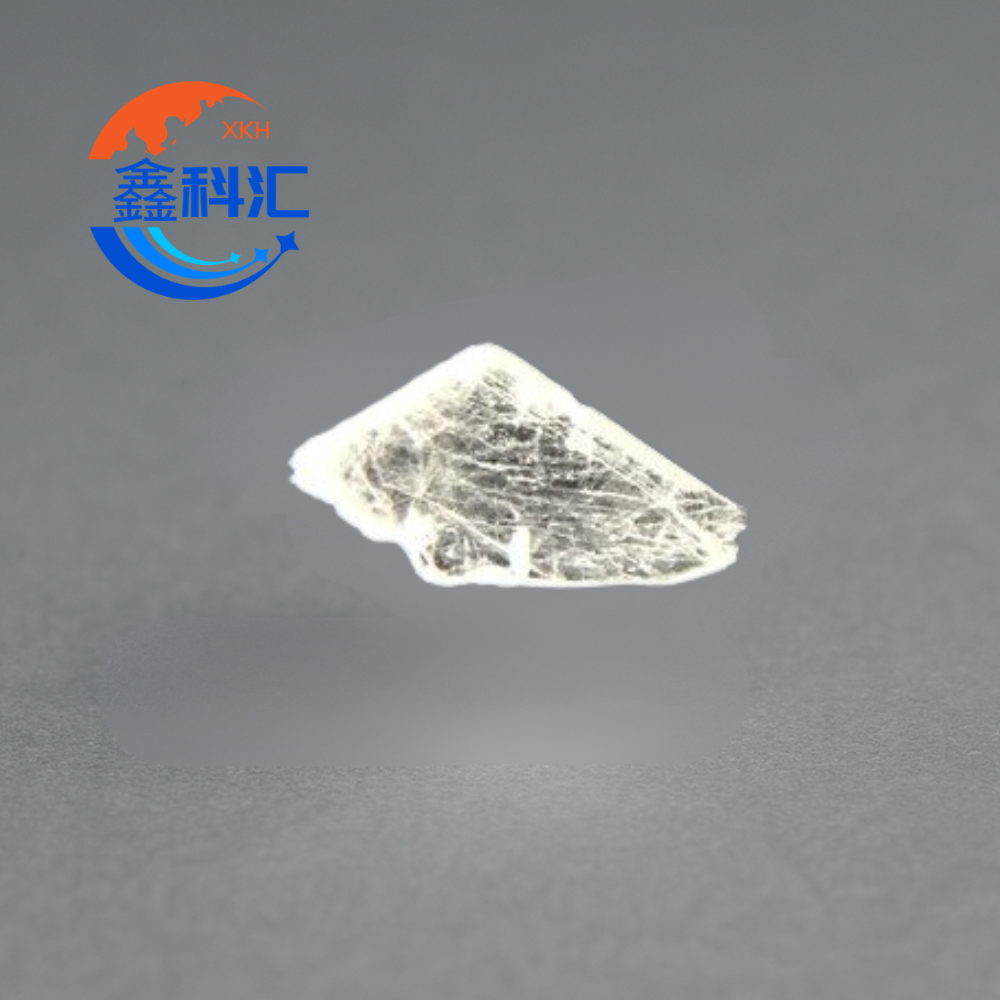
Understanding Hexagonal Boron Nitride
Hexagonal Boron Nitride (hBN) is a layered crystalline material composed of alternating boron and nitrogen atoms arranged in a hexagonal honeycomb lattice. Structurally, it resembles graphene, but its electronic properties are dramatically different.
While graphene is an excellent electrical conductor, hBN is an electrical insulator with a wide bandgap of approximately 6 eV. This unique combination of structural compatibility and electrical insulation makes hBN an ideal material for integrating with graphene and other two-dimensional materials.
Like graphite, hBN consists of atomically thin layers held together by weak van der Waals forces. These layers can be mechanically exfoliated to produce ultra-thin flakes suitable for device fabrication and scientific research.
What Does “Device-Grade” Mean?
Not all hBN crystals are created equal.
For many advanced applications, conventional polycrystalline boron nitride or lower-quality crystals are insufficient because defects, impurities, grain boundaries, and surface irregularities can significantly degrade device performance.
Device-grade hBN single crystals are specifically grown and selected to meet the demanding requirements of electronic and photonic devices. These materials typically feature:
- High crystal purity
- Low defect density
- Large single-crystal domains
- Atomically smooth surfaces
- Excellent dielectric properties
- Superior optical characteristics
The term “device-grade” indicates that the crystal quality is suitable for direct use in high-performance research and prototype devices rather than simply serving as a general engineering ceramic.
Why Is hBN So Important for Graphene Electronics?
One of the most influential discoveries in modern materials science is that graphene performs dramatically better when placed on hBN rather than conventional substrates such as silicon dioxide (SiO₂).
Graphene is highly sensitive to its surrounding environment. Surface roughness, trapped charges, and impurities can scatter electrons and reduce carrier mobility.
Device-grade hBN addresses these issues by providing:
- An atomically flat surface
- Extremely low surface charge disorder
- Excellent chemical stability
- Minimal contamination
As a result, graphene devices fabricated on hBN substrates often exhibit carrier mobilities many times higher than those fabricated on traditional dielectric materials.
This improvement allows researchers to explore fundamental quantum phenomena and develop higher-performance electronic devices.
Enabling Van der Waals Heterostructures
The rise of two-dimensional materials has led to the development of van der Waals heterostructures—artificially stacked layers of atomically thin materials with unique electronic and optical properties.
In these structures, hBN often serves as:
- A substrate layer
- An encapsulation layer
- An insulating spacer
- A tunnel barrier
Because hBN is atomically smooth and chemically inert, it preserves the intrinsic properties of neighboring materials while providing electrical isolation.
Today, many of the most advanced graphene, MoS₂, WS₂, and WSe₂ devices rely on hBN as a critical structural component.
Outstanding Electrical Properties
One reason hBN is highly valued in advanced electronics is its exceptional dielectric performance.
Device-grade hBN exhibits:
- High dielectric breakdown strength
- Low leakage current
- Excellent electrical insulation
- Stability under high electric fields
These properties make hBN an attractive material for nanoelectronics, high-frequency devices, and emerging quantum technologies where electrical reliability is essential.
As device dimensions continue to shrink, materials capable of maintaining strong insulating performance at the nanoscale become increasingly important.
A Promising Material for Quantum Technologies
Many of today’s most exciting developments in condensed matter physics and quantum electronics depend on ultra-clean material systems.
Researchers use device-grade hBN to create environments where electrons can move with minimal interference, enabling studies of:
- Quantum Hall effects
- Moiré superlattices
- Correlated electron systems
- Superconductivity
- Quantum transport phenomena
Because hBN introduces very few electronic disturbances, it has become a foundational material for experimental quantum devices.
Applications in Nanophotonics and Deep-UV Optoelectronics
Beyond electronics, hBN possesses remarkable optical properties.
The material supports phonon-polaritons, hybrid light-matter excitations that enable nanoscale manipulation of electromagnetic waves. This capability has generated significant interest in nanophotonics, optical metamaterials, and infrared technologies.
In addition, hBN exhibits deep ultraviolet (DUV) band-edge emission near 215 nm, making it a promising candidate for:
- UV light sources
- UV detectors
- Optical sensing systems
- Advanced photonic devices
As demand grows for compact ultraviolet technologies, hBN is expected to play an increasingly important role.
Challenges and Future Outlook
Despite its tremendous potential, large-scale production of high-quality hBN single crystals remains technically challenging.
Achieving large crystal sizes, low defect densities, and consistent quality requires sophisticated growth techniques and precise process control. As manufacturing technologies improve, the availability of device-grade hBN is expected to increase, supporting broader adoption across research and industry.
Many experts believe that hBN will remain a cornerstone material for future developments in quantum computing, advanced semiconductors, optoelectronics, and two-dimensional material systems.
Conclusion
Device-Grade hBN Single Crystal is far more than a specialty research material. Its unique combination of atomic flatness, electrical insulation, chemical stability, optical functionality, and compatibility with other two-dimensional materials makes it one of the most important enabling materials in modern electronics.
From graphene transistors and van der Waals heterostructures to quantum devices and deep-ultraviolet photonics, device-grade hBN continues to push the boundaries of what is possible in advanced technology. As the next generation of electronic and photonic systems emerges, the importance of high-quality hBN single crystals is only expected to grow.