
Wafer chucking force is one of the most important design parameters in semiconductor wafer handling, inspection, lithography, grinding, coating and precision machining equipment.
A 진공 척 must hold the wafer securely against acceleration, vibration and process loads. At the same time, it must avoid excessive local stress, backside contamination, wafer deformation and imprinting of the chuck surface pattern.
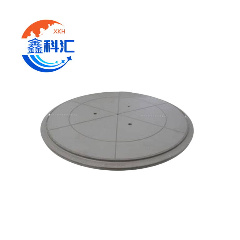
Increasing vacuum pressure does not automatically produce better wafer positioning. The final result depends on the interaction between:
- Vacuum pressure differential
- Effective vacuum area
- Actual wafer support area
- Vacuum groove or porous structure
- Wafer thickness and stiffness
- Initial wafer bow and warp
- Chuck surface flatness
- Backside particles
- Temperature distribution
- Vacuum leakage
Vacuum wafer chucks are widely used for wafer holding during processes including lithography, spin coating, etching, inspection and metrology. Ceramic chuck materials are often selected because they can provide high stiffness, dimensional stability, low thermal expansion and precision-machined surfaces.
This guide explains how vacuum pressure and contact geometry determine wafer chucking force, and how chuck design affects wafer flatness.
What Is Wafer Chucking Force?
Wafer chucking force is the net force pressing a wafer against the chuck surface.
For a vacuum chuck, the theoretical holding force can be estimated using:
F = ΔP × Aeff
Where:
- F is the theoretical chucking force
- ΔP is the pressure difference between atmospheric pressure and the pressure below the wafer
- Aeff is the effective sealed vacuum area
The pressure differential—not the vacuum pump specification alone—creates the holding force.
For example, a vacuum system may be described as operating at −60 kPa gauge pressure. Under normal atmospheric conditions, this represents an approximate pressure differential of 60 kPa between the upper and lower sides of the wafer.
However, the calculated value is only a theoretical maximum. The usable holding force can be lower because of:
- Leakage around the wafer edge
- Leakage through grooves or porous material
- Incomplete wafer-to-chuck sealing
- Vacuum line pressure loss
- Local wafer bow
- Surface particles
- Blocked vacuum channels
- Uneven pressure distribution
A practical design should therefore include an appropriate engineering safety factor rather than relying only on the ideal pressure-area calculation.
Vacuum Pressure vs Vacuum Flow
Vacuum pressure and vacuum flow are related, but they are not the same parameter.
Vacuum pressure
Vacuum pressure determines the pressure differential available to press the wafer against the chuck.
A larger pressure differential generally produces a larger theoretical chucking force.
Vacuum flow
Vacuum flow determines how quickly the system can evacuate air and how well it can compensate for leakage.
A system can show acceptable vacuum pressure when fully sealed but still respond slowly during wafer loading. Conversely, a high-flow pump may not achieve sufficient pressure differential if the wafer, chuck or tubing leaks excessively.
For this reason, vacuum chuck design should consider:
- Target vacuum pressure
- Required evacuation time
- Allowable leakage rate
- Vacuum port diameter
- Hose length and internal diameter
- Valve response time
- Groove resistance
- Porous ceramic permeability
- Wafer loading and release speed
For automated equipment, stable and repeatable pressure is usually more important than achieving the highest possible vacuum reading.
Effective Vacuum Area Is Not the Same as Contact Area
The term “contact area” can cause confusion in wafer chuck design.
There are two different areas that must be considered.
1. Effective vacuum area
The effective vacuum area is the projected sealed region over which the pressure differential acts.
This area primarily determines the theoretical chucking force.
If a 300 mm wafer covers a sealed vacuum region, the effective area may include much of the wafer footprint, even though only part of the wafer physically touches the chuck.
2. Physical support area
The physical support area is the actual solid-to-solid contact between the wafer backside and the chuck surface.
예를 들면 다음과 같습니다:
- Raised lands between vacuum grooves
- Pin tops on a pin chuck
- The surface network of a porous ceramic chuck
- Peripheral sealing rings
- Local support pads
Physical support area affects:
- Contact stress
- Friction
- Particle sensitivity
- Heat transfer
- Wafer deformation
- Backside marks
- Local flatness
- Release behavior
Therefore, increasing the physical support area does not necessarily increase the theoretical vacuum force. It changes how that force is transmitted into the wafer.
A chuck with a small support area may create high local contact pressure. A chuck with excessive support area may trap particles or increase wafer sticking. The correct design balances stable support with controlled vacuum distribution.
Example of Theoretical Chucking Force
Consider a 300 mm wafer with:
- Wafer radius: 0.15 m
- Pressure differential: 60 kPa
- Effective vacuum coverage: 65% of the wafer area
The full wafer area is approximately:
A = π × 0.15² = 0.0707 m²
The effective area is:
Aeff = 0.0707 × 0.65 = 0.0460 m²
The theoretical force is:
F = 60,000 × 0.0460 ≈ 2,760 N
This number should not be interpreted as the actual process holding force without further analysis.
The practical result depends on sealing, pressure uniformity, friction, groove configuration, wafer stiffness and process direction. In addition, the wafer may deform long before the theoretical maximum force is required.
How Vacuum Pressure Affects Wafer Flatness
Vacuum clamping can flatten a wafer with initial bow or warp by forcing it toward the chuck reference surface.
This can be useful in:
- 리소그래피
- 웨이퍼 검사
- 계측학
- Probing
- 그라인딩
- 다이싱
- 코팅
- Precision alignment
However, vacuum pressure can also create new deformation.
Research on precision pin chucks has shown that lift holes, ring seals and chuck features can cause local wafer deformation. Areas over openings may deflect differently from areas supported by pins or sealing structures, while the wafer edge may experience local buckling.
This means wafer flatness under vacuum is not determined only by the original wafer shape. It is the combined result of:
- Free-state wafer geometry
- Chuck surface geometry
- Support pattern
- Applied pressure differential
- Wafer bending stiffness
- Edge sealing
- Local openings
- Thermal conditions
A wafer may appear flat globally while still containing local high and low regions that affect focus, inspection accuracy or material removal uniformity.
Thin Wafers Are More Sensitive to Chucking Pressure
As wafer thickness decreases, resistance to bending decreases rapidly.
Thin wafers are therefore more likely to:
- Conform to chuck surface errors
- Sag into wide grooves
- Deflect over vacuum ports
- Show pin-pattern print-through
- Develop edge distortion
- Crack during rapid clamping
- Stick during release
- Respond strongly to backside particles
This is especially important for:
- Back-ground silicon wafers
- Compound semiconductor wafers
- Glass wafers
- 사파이어 웨이퍼
- SiC 웨이퍼
- SOI wafers
- MEMS substrates
- Temporary-bonded wafers
- Reconstituted or molded wafers
A vacuum pressure that works well for a standard-thickness silicon wafer may be excessive for an ultra-thin wafer.
The chuck should therefore be evaluated using the actual wafer thickness, material, diameter, edge condition and expected bow—not only the nominal wafer size.
How Groove Design Influences Chucking Force
Grooved vacuum chucks use machined channels to distribute vacuum below the wafer.
Common configurations include:
- Concentric circular grooves
- Radial grooves
- Spiral grooves
- Cross-grid grooves
- Zoned vacuum channels
- Independent inner and outer circuits
- Edge sealing rings
Groove width
Wide grooves can improve air evacuation but provide less support beneath the wafer. If the unsupported span is too large, a thin wafer may sag into the groove.
Groove depth
Deeper grooves increase internal flow volume but may slow pressure stabilization. Excessively deep features may also make cleaning more difficult.
Groove spacing
Closely spaced grooves can improve pressure distribution, but they also create more edges where particles can accumulate.
Vacuum port location
A single central port may produce uneven evacuation in a large chuck if the channel resistance is high.
Multiple ports or balanced distribution networks can reduce pressure differences across the chuck.
Zoned vacuum
Separate vacuum zones can be useful when the equipment handles different wafer diameters or when sequential clamping is required.
However, zone boundaries must be designed carefully because pressure discontinuities can introduce local deformation.
Porous Ceramic Vacuum Chucks
Porous ceramic chucks distribute vacuum through a network of interconnected pores rather than relying only on large machined grooves.
Porous ceramic properties such as porosity and pore diameter can be controlled for the intended gas-flow requirement. These materials are used in vacuum chuck applications because gases can pass through the ceramic structure while the surface provides distributed wafer support.
잠재적인 장점으로는 다음과 같은 것들이 있습니다:
- More uniform vacuum distribution
- Reduced dependence on large grooves
- Lower risk of visible groove print-through
- Support across a broad surface
- Stable handling of thin substrates
- Simplified surface pattern
Important design factors include:
- Average pore size
- Porosity
- Air permeability
- Surface flatness
- 표면 거칠기
- Porous layer thickness
- Base material
- Bonding structure
- Cleaning method
- 파티클 생성
- Vacuum response time
A porous chuck is not automatically suitable for every process. Extremely high permeability may increase vacuum demand, while low permeability may result in slow clamping.
The porous structure must be matched to the pump capacity, wafer backside condition and required response time.
Pin Chucks and Local Wafer Deformation
A pin chuck supports the wafer on an array of small raised pins.
Pin chucks can reduce the total solid contact area and lower sensitivity to some types of backside contamination. However, each pin creates a discrete support point.
The resulting wafer shape depends on:
- Pin diameter
- Pin pitch
- Pin height consistency
- Vacuum pressure
- Wafer thickness
- Lift-hole diameter
- Peripheral sealing design
- Pin surface condition
If pin spacing is too large, the wafer may deflect between pins. If pin height variation is excessive, the wafer may follow the pin-height error.
Lift holes and sealing rings are particularly important because they interrupt the regular support pattern. Published finite-element studies have demonstrated that these features can degrade local wafer flatness under vacuum.
Chuck Surface Flatness and Wafer Flatness
A vacuum chuck cannot consistently produce a wafer surface flatter than the combined performance of:
- Chuck reference surface
- Support-point uniformity
- Machine mounting surface
- Wafer backside cleanliness
- Vacuum distribution
- 열 안정성
- Measurement method
High-precision ceramic vacuum chucks are used because ceramic materials can provide high stiffness, low thermal expansion and precision-machined surface profiles. Commercial ceramic chucks are available in materials including alumina, silicon carbide, porous ceramics and cordierite.
However, chuck flatness should not be specified without defining the measurement condition.
An RFQ should clarify whether flatness is measured:
- Before or after installation
- With or without vacuum
- At room temperature or operating temperature
- Across the full diameter
- Inside an edge exclusion zone
- On the support lands
- On a reference plane
- With the wafer loaded
- Using optical, capacitive or contact measurement
A chuck can meet a free-state flatness specification but distort after mounting if bolt torque, base-plate flatness or thermal expansion is not controlled.
Backside Particles and Contact Stress
A particle trapped between the wafer and chuck acts as a local high point.
When vacuum is applied, the wafer is pressed against the particle. This may cause:
- Local wafer deformation
- Backside scratches
- Front-side focus error
- Wafer rocking
- Particle transfer
- Wafer cracking
- Nonuniform grinding or polishing
Higher vacuum pressure increases the force transmitted through the particle.
Particle sensitivity is influenced by the support pattern. A dense contact surface may trap a particle beneath the wafer, while a pin or porous structure may reduce or redistribute the effect depending on where the particle lands.
The chuck design should include an appropriate cleaning and inspection strategy, particularly for high-flatness applications.
Friction and Resistance to Lateral Movement
Vacuum force acts mainly normal to the chuck surface.
Resistance to lateral wafer movement depends largely on friction:
Flateral ≈ μ × Fnormal
Where:
- μ is the effective friction coefficient
- Fnormal is the total normal clamping force
The effective friction coefficient can change because of:
- Wafer backside coating
- Moisture
- 표면 거칠기
- Contamination
- Chuck material
- 온도
- Process gas
- Contact-area distribution
For processes involving high acceleration, spindle rotation or lateral cutting forces, the design should verify both normal holding force and lateral slip resistance.
Simply calculating the vertical vacuum force is not sufficient.
Thermal Effects on Wafer Chucking
Temperature changes can alter both the chuck and wafer geometry.
Relevant factors include:
- Chuck thermal expansion
- Wafer thermal expansion
- Radial temperature gradients
- Local heating from the process
- Cooling-channel layout
- Vacuum-dependent thermal contact
- Material thermal conductivity
- Base-plate expansion
Vacuum clamping restricts some wafer movement. As a result, thermal deformation under chucking conditions may differ from the wafer’s free thermal deformation. Numerical studies of vacuum-clamped wafers have shown that chucking influences wafer warpage and local thermal distortion.
For temperature-sensitive processes, flatness should be evaluated at the actual operating temperature rather than only at room temperature.
Common Problems and Likely Causes
The wafer moves during processing
Possible causes:
- Insufficient pressure differential
- Low effective vacuum area
- Excessive leakage
- Low surface friction
- Blocked grooves
- Undersized vacuum lines
- Excessive process acceleration
The wafer is flat at low vacuum but distorted at high vacuum
Possible causes:
- Excessive chucking pressure
- Wide groove spacing
- Large unsupported openings
- Uneven pin height
- Ring-seal deformation
- Chuck surface error
- Backside particles
Vacuum pressure is unstable
Possible causes:
- Edge leakage
- Warped wafer
- Damaged sealing ring
- Porous material contamination
- Loose fittings
- Insufficient pump flow
- Valve instability
The wafer is difficult to release
Possible causes:
- Residual vacuum
- Slow venting
- Excessive contact area
- Moisture adhesion
- 정전기 인력
- 표면 오염
- Inadequate blow-off design
Different wafers show different flatness results
Possible causes:
- Variation in wafer bow or warp
- Different wafer thickness
- Backside film differences
- Edge-shape variation
- 입자 오염
- Changes in vacuum pressure
- Temperature variation
Wafer Chuck Design Workflow
A practical development process should follow several steps.
Step 1: Define the wafer
Specify:
- Wafer material
- Diameter
- 두께
- Bow
- Warp
- TTV
- Edge profile
- Backside coating
- Surface sensitivity
Step 2: Define process loads
Specify:
- Maximum acceleration
- Rotational speed
- Lateral process force
- Vertical force
- Vibration
- Process temperature
- Required positioning repeatability
Step 3: Calculate the required holding force
Estimate the normal and lateral force requirements, then include a suitable safety factor.
Do not select vacuum pressure only from previous equipment experience.
Step 4: Select the support structure
Compare:
- Grooved dense ceramic chuck
- Porous ceramic chuck
- Pin chuck
- Multi-zone chuck
- Hybrid porous-and-grooved structure
Step 5: Model wafer deformation
For precision applications, use finite-element analysis to evaluate:
- Pressure-induced wafer deformation
- Groove print-through
- Lift-hole deformation
- Pin spacing
- Edge buckling
- Thermal distortion
- Mounting stress
Step 6: Validate with actual wafers
Test:
- Evacuation time
- Vacuum stability
- Holding force
- Lateral slip
- Loaded wafer flatness
- Wafer release
- Particle performance
- Repeatability
- 열 순환
RFQ Checklist for a Custom Ceramic Wafer Chuck
To obtain an accurate quotation, provide the following information.
Wafer information
- Wafer material
- 웨이퍼 직경
- Wafer thickness range
- Bow and warp range
- TTV requirement
- Backside condition
- Edge exclusion
Chuck dimensions
- Outer diameter
- Overall thickness
- Mounting-hole pattern
- Central opening
- Lift-pin holes
- Alignment features
- Vacuum port position
Vacuum requirements
- Operating vacuum pressure
- Pump flow capacity
- Maximum allowable leakage
- Required chucking time
- Required release time
- Number of vacuum zones
- Blow-off requirement
Surface requirements
- Chuck flatness
- 병렬 처리
- 표면 거칠기
- Groove width and depth
- Porous area
- Edge seal
- Allowable particle level
재료 요구 사항
- 알루미나
- 실리콘 카바이드
- Porous alumina
- Porous silicon carbide
- Cordierite
- 질화알루미늄
- Other technical ceramic
Operating conditions
- Process temperature
- 화학 물질 노출
- 플라즈마 노출
- Cleanroom level
- Mechanical load
- 열 순환
- Electrical resistivity requirement
- Static-dissipation requirement
Inspection requirements
- Flatness report
- Dimensional report
- Material certificate
- Surface roughness report
- Airflow or permeability test
- Vacuum leakage test
- Cleaning and packaging standard
자주 묻는 질문
Does higher vacuum always improve wafer flatness?
No. Higher vacuum can flatten initial wafer bow, but it can also increase local deformation over grooves, pins, lift holes, particles and sealing structures.
What determines vacuum chucking force?
The primary factors are pressure differential and effective sealed vacuum area. Leakage, pressure distribution and wafer sealing reduce the practical force.
Does a larger contact area increase chucking force?
Not directly. The theoretical vacuum force depends primarily on pressure differential and effective vacuum area. Physical contact area affects stress distribution, friction, heat transfer and wafer deformation.
Why does a thin wafer sag into vacuum grooves?
A thin wafer has lower bending stiffness. If the groove width or support spacing is too large, vacuum pressure can pull the wafer into the unsupported region.
Is a porous ceramic chuck better than a grooved chuck?
It depends on the process. Porous chucks can provide distributed vacuum and broad support, while grooved chucks may offer easier control of vacuum zones and flow paths. The best choice depends on wafer thickness, cleanliness, response time and flatness requirements.
Which ceramic material is suitable for a vacuum wafer chuck?
Alumina is commonly used for electrical insulation and precision ceramic components. Silicon carbide is attractive where high stiffness, thermal conductivity and dimensional stability are important. Porous ceramics are used when distributed airflow is required. Final material selection should be based on the operating environment and precision requirements.
What information is most important when ordering a custom chuck?
The supplier should receive the wafer diameter, thickness, bow and warp, required loaded flatness, vacuum pressure, chuck dimensions, surface pattern, material, operating temperature and inspection requirements.
결론
Wafer chucking force should not be treated as a simple vacuum-pressure specification.
The theoretical holding force is determined by pressure differential and effective vacuum area, but wafer performance is controlled by the complete mechanical system.
The most important relationships are:
- Vacuum pressure determines the available normal force.
- Effective vacuum area determines how much of that pressure produces holding force.
- Physical contact area determines how the force is transferred to the wafer.
- Groove, pin and porous structures determine local pressure and support distribution.
- Wafer thickness and material determine sensitivity to deformation.
- Chuck flatness, mounting and particles determine actual loaded wafer geometry.
- Excessive vacuum can reduce rather than improve local flatness.
For high-precision semiconductor equipment, the chuck should be designed and tested using the actual wafer, vacuum condition, temperature and process load.
A well-designed ceramic vacuum chuck must provide sufficient holding force while maintaining wafer flatness, cleanliness, repeatability and reliable release.

