As semiconductor technology continues to scale beyond traditional silicon-based architectures, the industry is increasingly turning toward new classes of materials that can support higher performance, lower power consumption, and fundamentally new device physics. Among these emerging materials, device-grade hexagonal boron nitride (hBN) single crystal has rapidly gained attention as a strategic enabler for next-generation electronics.
Once considered a niche laboratory material, hBN is now recognized as a critical component in advanced semiconductor research, particularly in two-dimensional (2D) electronics, quantum devices, and van der Waals heterostructures.
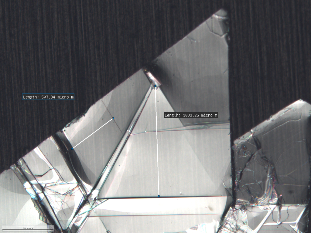
The Semiconductor Industry Is Facing Fundamental Limits
Modern semiconductor scaling is approaching physical and material constraints. As device dimensions shrink, several challenges become increasingly severe:
- Increased electron scattering at interfaces
- Rising power density and thermal management issues
- Material incompatibility at atomic scales
- Quantum interference effects in ultra-small devices
- Degradation of carrier mobility in advanced channels
These limitations are driving the search for new materials that can operate reliably at the nanoscale while preserving electronic performance.
What Makes hBN a Strategic Material?
Hexagonal boron nitride (hBN) is a layered wide-bandgap material with a crystal structure similar to graphene. However, its electronic properties are fundamentally different: it is an excellent electrical insulator with exceptional chemical and thermal stability.
Amikor a következő formában készül: device-grade singlecrystals, hBN exhibits properties that are highly desirable for semiconductor applications:
- Atomically flat surface morphology
- Ultra-low charge trap density
- High dielectric breakdown strength (~1.6 V/nm typical)
- Széles sávrés (~6 eV)
- Strong chemical inertness
- Van der Waals-féle felületi kompatibilitás
These characteristics make hBN uniquely suited for integration into advanced device architectures.
Enabling High-Performance 2D Semiconductor Platforms
One of the most important roles of hBN in future electronics is its function as a substrate and encapsulation material for two-dimensional systems.
In 2D semiconductors such as graphene, MoS₂, WS₂, and WSe₂, device performance is highly sensitive to the surrounding environment. Conventional substrates introduce disorder, charge traps, and surface roughness, all of which degrade electronic properties.
Device-grade hBN solves these issues by providing:
- A chemically inert and clean interface
- Minimális elektrosztatikus zavar
- Atomically smooth support layers
- Csökkentett fonon-szórás
As a result, 2D devices built on hBN demonstrate significantly improved mobility, stability, and reproducibility.
The Role of hBN in Van der Waals Heterostructures
A major breakthrough in modern materials science is the concept of van der Waals-heterostruktúrák, where atomically thin layers of different materials are stacked without requiring lattice matching.
In this architecture, hBN plays multiple critical roles:
- Substrate layer for 2D materials
- Encapsulation layer for device protection
- Dielectric spacer in tunnel devices
- Insulating barrier in quantum structures
Its structural compatibility with graphene and other layered materials makes hBN the “universal interface material” for 2D device engineering.
Enabling Quantum and Ballistic Transport Devices
As semiconductor devices enter the quantum regime, controlling disorder at the atomic scale becomes essential. Device-grade hBN single crystals are particularly important in this context.
By minimizing charge fluctuations and surface imperfections, hBN enables:
- High-mobility electron transport
- Observation of quantum Hall effects
- Ballistic transport over micrometer scales
- Formation of moiré superlattices
- Stable quantum coherence in low-dimensional systems
These properties are essential for emerging quantum electronics and fundamental physics research.
Thermal and Electrical Advantages in Device Scaling
Beyond electronic quality, hBN also provides strong thermal and dielectric advantages:
- Efficient heat dissipation in nanoscale structures
- High dielectric strength for insulating layers
- Stabilitás erős elektromos mezőkben
- Resistance to chemical and environmental degradation
These properties are increasingly important as device architectures become more complex and power-dense.
Why “Device-Grade” Matters
Not all hBN materials are suitable for semiconductor applications. Polycrystalline or low-quality BN materials introduce grain boundaries, impurities, and structural defects that significantly degrade device performance.
Device-grade hBN single crystals are defined by:
- Nagy egykristályos tartományok
- Extremely low defect density
- High structural uniformity
- Atomszinten sima felületek
- Reproducible electronic performance
This level of material quality is essential for advanced semiconductor research and prototype device fabrication.
Strategic Importance in Future Semiconductor Ecosystems
Device-grade hBN is increasingly seen as a foundational material in several key technological directions:
- 2D semiconductor electronics
- Quantum computing hardware
- Advanced RF and high-frequency devices
- Nanoscale photonic systems
- Ultra-low-power electronic architectures
Rather than being a passive insulating layer, hBN is now recognized as an active enabler of performance in next-generation device stacks.
Következtetés
Device-grade hBN single crystals are becoming a strategic material for future semiconductors because they address some of the most fundamental challenges in nanoscale electronics: disorder, interface quality, and material compatibility.
By providing an atomically perfect, electrically inert, and structurally compatible platform for two-dimensional materials, hBN enables performance levels that are not achievable with conventional semiconductor substrates.
As the semiconductor industry continues to evolve toward quantum and atomically engineered systems, device-grade hBN is expected to play an increasingly central role in defining the future of electronics.