
Structural ceramics play a critical role in semiconductor manufacturing equipment because many process components must operate under conditions that are difficult for conventional metals and polymers.
Depending on the process, equipment parts may be exposed to:
- Plasma and reactive process gases
- High or rapidly changing temperatures
- Vákuumos környezet
- Radio-frequency and microwave energy
- Aggressive chamber-cleaning chemistry
- Repeated wafer-transfer cycles
- Tight flatness and positioning requirements
- Strict particle and metallic-contamination limits
- Electrical insulation or controlled conductivity requirements
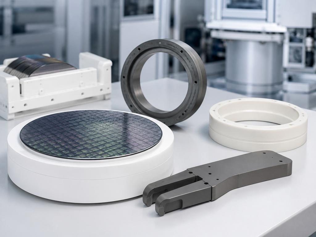
Advanced ceramics are used in wafer handling, lithography, etching, deposition, thermal processing, cleaning, inspection, back grinding and other semiconductor processes. Ceramic components commonly include vacuum chucks, electrostatic chuck parts, end effectors, focus rings, chamber liners, nozzles, showerheads, heater components, wafer boats and precision stage structures.
However, “ceramic” is not a single material specification.
Alumina, silicon carbide, aluminum nitride, silicon nitride, zirconia, yttria and cordierite have very different mechanical, thermal, electrical and plasma-resistance characteristics. Material grade, purity, porosity, additives, forming method and surface condition can also affect performance.
This guide explains how to select structural ceramic components and materials for semiconductor manufacturing equipment.
What Are Structural Ceramics?
Structural ceramics are engineered ceramic materials used primarily for their mechanical, thermal, dimensional, chemical or wear-related properties.
Unlike a ceramic electronic package or dielectric substrate whose main purpose may be electrical interconnection, a structural ceramic component generally performs one or more physical equipment functions:
- Supporting a wafer
- Positioning a process component
- Carrying mechanical load
- Maintaining flatness
- Resisting chamber erosion
- Isolating electrical potential
- Distributing process gas
- Conducting or insulating heat
- Guiding wafer movement
- Maintaining dimensions during temperature changes
Some semiconductor components combine structural and functional requirements.
For example, an electrostatic chuck body must provide mechanical flatness, electrical behavior, thermal control and vacuum compatibility. A plasma window must resist chemical erosion while transmitting radio-frequency or microwave energy with controlled dielectric loss.
Fine ceramics include a broad range of engineered materials, and their properties can be adjusted through raw-material selection, particle size, additives and firing methods. This makes material grade selection just as important as choosing the general ceramic family.
Why Semiconductor Equipment Uses Structural Ceramics
Structural ceramics are selected when an equipment component requires a combination of properties that is difficult to obtain from metal, glass or polymer materials.
Important ceramic characteristics may include:
- Nagy keménység
- Nagy merevség
- Alacsony hőtágulás
- Elektromos szigetelés
- Ellenőrzött elektromos ellenállás
- High-temperature strength
- Plazma ellenállás
- Kémiai ellenállás
- Kopásállóság
- Méretbeli stabilitás
- Alacsony részecskeképződés
- High-purity composition
- Vákuum kompatibilitás
Kyocera identifies high precision, mechanical performance, heat resistance, plasma resistance, low particle generation and low dielectric loss as important requirements for ceramic components used in semiconductor processing equipment.
The required combination changes significantly from one process to another. A material suitable for a robot end effector may not be the best material for an etch focus ring, heater plate or high-temperature wafer boat.
Main Structural Ceramic Components in Semiconductor Equipment
Ceramic parts are used throughout front-end and back-end semiconductor manufacturing equipment.
Wafer kezelő alkatrészek
Wafer handling components move wafers between load ports, cassettes, aligners, process chambers and inspection stations.
A tipikus kerámia alkatrészek közé tartoznak:
- Wafer end effectors
- Robot blades
- Wafer transfer arms
- Edge-gripping components
- Vacuum pickup pads
- Lift pins
- Alignment pins
- Wafer vezetők
- Support pads
- Vákuum tokmányok
Wafer-handling parts require high dimensional precision, controlled weight, sufficient stiffness and clean wafer-contact surfaces. Depending on the application, they may also require electrical insulation or static-dissipative properties.
High-purity alumina, silicon carbide and other semiconductor-grade ceramics are used for wafer handling because they can provide abrasion resistance, dimensional stability and controlled surface performance.
Important selection factors
- Wafer diameter and thickness
- Robot speed and acceleration
- Maximum end-effector mass
- Blade deflection
- Contact-pad flatness
- Wafer backside sensitivity
- Vacuum pressure and leakage
- Electrical resistivity
- Particle-generation limits
- Tisztítási előírások
For high-speed and long-reach robot arms, specific stiffness—the relationship between elastic modulus and density—is often more important than either stiffness or density considered separately.
Vacuum Chucks and Precision Wafer Stages
Vacuum chucks hold wafers during:
- Ellenőrzés
- Metrológia
- Litográfia
- Dicing
- Back grinding
- Bevonat
- Alignment
- Precision machining
Ceramic vacuum chucks may use:
- Machined vacuum grooves
- Porous ceramic surfaces
- Pin-support structures
- Independent vacuum zones
- Peripheral sealing lands
The chuck must provide sufficient holding force while controlling wafer deformation, backside particles and release behavior.
Kyocera supplies high-precision ceramic vacuum chucks with different surface patterns for wafer holding and transport. The same type of ceramic technology is also used for precision stage components in lithography and inspection equipment.
Critical design requirements
- Chuck surface flatness
- Parallelism to the mounting datum
- Felület érdessége
- Vacuum-groove geometry
- Porous-material permeability
- Effective vacuum area
- Wafer edge exclusion
- Hőtágulás
- Mounting-induced distortion
- Electrical resistance
- Cleaning and packaging
A ceramic chuck should not be specified only by outside diameter and flatness. The supplier also needs the wafer thickness, bow, warp, operating pressure, temperature and loaded-flatness requirement.
Electrostatic Chuck Components
Electrostatic chucks use electrostatic force to hold a wafer during etching, deposition, implantation and other processes.
Ceramic portions of an electrostatic chuck may be required to provide:
- Wafer support and flatness correction
- Elektromos szigetelés
- Ellenőrzött elektromos ellenállás
- Embedded electrode insulation
- Thermal conduction
- Gas-channel integration
- Plazma ellenállás
- Méretbeli stabilitás
Electrostatic chucks are also used to support wafer cooling during semiconductor processing.
Common material candidates include:
- Alumina
- Alumínium-nitrid
- Controlled-resistivity ceramics
- Ceramic coatings
- Composite ceramic structures
The exact ceramic grade must be selected according to chucking method, voltage, process temperature, backside cooling gas, plasma exposure and electrical-resistance requirements.
Etch Chamber Components
Plasma etching exposes chamber parts to reactive gases, ion bombardment, RF energy, volatile byproducts and repeated chamber-cleaning cycles.
A tipikus kerámia alkatrészek közé tartoznak:
- Fókuszgyűrűk
- Peremgyűrűk
- Fúvókák
- Gas injectors
- Showerheads
- Chamber windows
- Chamber lids
- Shields
- Liners
- Szigetelők
- Plasma-resistant domes
Focus and edge rings help control conditions around the wafer perimeter. Nozzles and injectors distribute process gases, while dielectric windows may transmit RF or microwave energy into the plasma chamber.
These parts require combinations of:
- Plasma erosion resistance
- Nagy tisztaság
- Chemical compatibility
- Áramszigetelési szilárdság
- Alacsony dielektromos veszteség
- Méretbeli stabilitás
- Alacsony részecskeképződés
CoorsTek lists focus rings, nozzles, windows, lids, shields and showerheads among the ceramic components used in plasma-etch equipment.
Deposition Chamber Components
Chemical vapor deposition, physical vapor deposition, atomic layer deposition and related processes may combine:
- Reactive precursor gases
- Plasma
- Elevated temperatures
- Vacuum
- Repeated cleaning chemistry
Ceramic deposition components include:
- Chamber domes
- Kamrabélések
- Deposition rings
- Gázelosztó lemezek
- Showerheads
- Pedestal-heater components
- Plating insulators
- Vacuum-break filters
- Electrical isolators
Deposition rings and chamber liners are directly exposed to the process environment, making purity, plasma durability and resistance to coating buildup important.
High-purity alumina, aluminum nitride, silicon carbide and plasma-resistant coatings are among the material systems used for deposition equipment.
Ceramic Heaters and Pedestal Components
Ceramic heaters may integrate a resistive heating element within a ceramic body.
Az alkalmazások közé tartoznak:
- Wafer heating
- Temperature-controlled process pedestals
- Vacuum heating
- Deposition equipment
- Etch equipment
- Analytical equipment
The ceramic body may need to provide:
- Elektromos szigetelés
- Uniform heat distribution
- Controlled thermal expansion
- Mechanical flatness
- Thermal-cycle resistance
- Vákuum kompatibilitás
- Gas-channel integration
Aluminum nitride is often considered for heater and pedestal applications because it combines electrical insulation with relatively high thermal conductivity. Alumina can also be appropriate when temperature, thermal-uniformity and cost requirements permit.
Wafer Boats and High-Temperature Fixtures
Ceramic wafer boats, carriers and furnace fixtures support wafers during thermal processing.
These components may be exposed to:
- High temperature
- Repeated heating and cooling
- Process gases
- Mechanikai terhelés
- Long service cycles
- Wafer-contact cleanliness requirements
Typical ceramic materials include:
- Nagy tisztaságú alumínium-oxid
- Szilícium-karbid
- Recrystallized silicon carbide
- Reaction-bonded silicon carbide
- CVD-coated silicon carbide
- Sapphire for selected applications
The material and design must account for:
- Maximális üzemi hőmérséklet
- Thermal gradients
- Wafer size
- Slot spacing
- Carrier orientation
- Process-gas chemistry
- Allowable contamination
- Thermal mass
- Dimensional change over service life
Alumina wafer boats are used because of their heat, wear and chemical resistance, while SiC materials may be selected when higher thermal conductivity, rigidity or high-temperature strength is required.
Inspection, Metrology and Lithography Components
Semiconductor inspection and lithography equipment require accurate positioning and stable dimensions.
Ceramic components may include:
- Precíziós szakaszok
- Stage bases
- Integrated mirror structures
- Wafer chucks
- Guide components
- Probe-card components
- Alignment structures
- Cutter and grinder components
- Metrology frames
These applications often prioritize:
- Nagy merevség
- Low moving mass
- Alacsony hőtágulás
- Vibration stability
- High surface accuracy
- Repeatable mounting
- Hosszú távú méretstabilitás
Cordierite and silicon carbide can be considered for lightweight precision structures, while alumina is frequently used for insulating and general precision components.
Kyocera reports that precision ceramic components are used in probers, wafer cutters, back grinders, inspection equipment and wafer-transfer systems.
Structural Ceramic Material Selection
Material selection should start with the component’s actual operating conditions rather than with a preferred material name.
Alumina
Alumina, or aluminum oxide, is one of the most widely used technical ceramics.
Its general advantages include:
- Jó mechanikai szilárdság
- Nagy keménység
- Elektromos szigetelés
- Kopásállóság
- Kémiai ellenállás
- Availability in multiple purity grades
- Established precision-machining methods
- Competitive cost relative to many specialized ceramics
Higher-purity alumina grades are often selected for semiconductor chamber components because they provide improved corrosion, wear and contamination performance compared with lower-purity industrial grades.
Common semiconductor applications
- Elektromos szigetelők
- Robot blades
- Fúvókák
- Kamrabélések
- Wafer csónakok
- Vacuum components
- Heater bodies
- Lift pins
- Mechanical supports
- Gas-distribution parts
Important limitations
- Higher thermal expansion than some SiC grades
- Lower thermal conductivity than AlN and many SiC materials
- Brittle response at sharp corners and thin sections
- Standard grades may not provide sufficient plasma resistance for demanding chamber locations
- Electrically insulating alumina may retain static charge unless an ESD-safe grade or coating is used
The RFQ should state the required alumina purity rather than simply specifying “alumina ceramic.”
Szilícium-karbid
Silicon carbide offers a strong combination of:
- Nagy keménység
- Nagy merevség
- Relatively low density
- Nagy hővezető képesség
- Alacsony hőtágulás
- High-temperature strength
- Kopásállóság
- Kémiai ellenállás
Kyocera identifies SiC as a hard, chemically resistant ceramic with high thermal conductivity and strength retention at elevated temperatures.
Common semiconductor applications
- Wafer end effectors
- Precíziós szakaszok
- Vákuum tokmányok
- Fókuszgyűrűk
- Peremgyűrűk
- Szuszceptorok
- Magas hőmérsékletű szerelvények
- Wafer csónakok
- Kamrai alkatrészek
- CVD or epitaxy components
SiC grade differences
The term “silicon carbide” may refer to several different material systems:
- Pressureless-sintered SiC
- Reaction-bonded SiC
- Silicon-infiltrated SiC
- Átkristályosított SiC
- CVD SiC
- CVD-coated graphite
- CVD-coated bulk SiC
These grades differ in:
- Free-silicon content
- Sűrűség
- Porosity
- Tisztaság
- Electrical resistivity
- Hővezető képesség
- Oxidation behavior
- Plazma ellenállás
- Machining method
- Maximum practical component size
A reaction-bonded SiC component containing residual silicon should not automatically be treated as equivalent to high-purity sintered or CVD SiC.
CVD Silicon Carbide
Chemical vapor deposited silicon carbide may be supplied as:
- Free-standing CVD SiC
- A CVD SiC coating on graphite
- A CVD SiC coating on another SiC substrate
CVD SiC is used in demanding semiconductor environments requiring high purity, corrosion resistance, wear resistance, oxidation resistance and high-temperature performance.
Potential applications
- Plasma-exposed rings
- Chamber components
- Epitaxy susceptors
- High-purity liners
- Thin-wall process parts
- Protective coatings
- Components exposed to aggressive process chemistry
The substrate, coating thickness, coating continuity and thermal-expansion relationship must all be considered when CVD SiC is used as a coating rather than as a free-standing part.
Alumínium-nitrid
Az alumínium-nitrid kombinálódik:
- Elektromos szigetelés
- Relatively high thermal conductivity
- Moderate thermal expansion
- Hőstabilitás
- Compatibility with integrated heating structures
Unlike many electrically insulating ceramics, AlN can transfer heat efficiently while maintaining electrical isolation.
Common semiconductor applications
- Kerámia fűtőtestek
- Electrostatic chuck bodies
- Pedestal components
- Thermal-management parts
- Elektromos szigetelők
- High-temperature wafer-support components
- Heat-spreading structures
Important limitations
- Material properties vary significantly by grade
- Moisture and cleaning-chemistry compatibility require review
- Machining and finishing can be more demanding than for common alumina grades
- Surface oxidation and long-term environmental exposure should be evaluated
- Cost is generally higher than standard alumina
AlN should be selected when its thermal and electrical combination is necessary, not simply because it is considered a more advanced ceramic.
Szilícium-nitrid
Silicon nitride is known for:
- Nagy mechanikai szilárdság
- Improved fracture resistance compared with many conventional ceramics
- Kopásállóság
- Alacsony hőtágulás
- Thermal-shock resistance
- Strength retention at elevated temperatures
Kyocera describes silicon nitride as a high-strength ceramic with strong wear and thermal-shock performance.
Potential semiconductor applications
- Mechanically loaded support components
- Lift pins
- Wear components
- Precision moving parts
- Thin structural features
- Components exposed to repeated temperature changes
- Selected focus rings and chamber parts
Silicon nitride may be valuable where mechanical shock and fracture risk are more important than maximum stiffness or thermal conductivity.
Cirkónia
Zirconia offers:
- Nagy törési szívósság
- High strength
- Kopásállóság
- Good surface finish
- Resistance to local mechanical damage
Compared with alumina and SiC, zirconia generally has:
- Higher density
- Lower stiffness
- Nagyobb hőtágulás
- Alacsonyabb hővezető képesség
Potential semiconductor applications
- Wear pads
- Small alignment parts
- Szelep alkatrészek
- Precision plungers
- Mechanical inserts
- Contact tips
- Components requiring greater resistance to chipping
Zirconia is often more suitable for small wear-resistant or mechanically sensitive components than for large lightweight stage structures or robot arms.
Yttria
Yttria, or yttrium oxide, is particularly important for plasma-exposed components.
Its principal benefit is strong resistance to plasma corrosion, which can help reduce the generation of particles and unwanted impurities in semiconductor plasma processes.
Yttria may be used as:
- A bulk ceramic
- A coating on alumina
- A coating on aluminum nitride
- A chamber-protection layer
- A plasma-facing surface
Typical applications
- Etch chamber liners
- Plasma-resistant rings
- Domes
- Shields
- Chamber walls
- Fúvókák
- Coated electrostatic chuck parts
A yttria coating must be evaluated for:
- Coating thickness
- Adhesion
- Porosity
- Felületkezelés
- Plasma-erosion uniformity
- Edge coverage
- Termikus ciklikusság
- Cleaning compatibility
- Particle shedding
Bulk yttria and yttria coatings do not necessarily provide identical performance.
Cordierite
Cordierite has an extremely low coefficient of thermal expansion and can provide good dimensional stability under temperature change.
It is used for structural parts in semiconductor equipment and precision optical structures where low thermal distortion is important.
Potential applications
- Precíziós szakaszok
- Metrology structures
- Mirror substrates
- Inspection-equipment components
- Thermally stable support frames
Cordierite is not usually selected for the most aggressive plasma or wear environments. Its primary value is thermal dimensional stability.
Porózus kerámia
Porous ceramics contain a controlled network of pores that allows gas flow through the material.
In semiconductor equipment, they may be used for:
- Vákuum tokmányok
- Wafer-support surfaces
- Gas-distribution components
- Vacuum-break filters
- Air-bearing or handling functions
Important porous-material specifications include:
- Average pore size
- Pore-size distribution
- Porosity
- Air permeability
- Felületi simaság
- Felület érdessége
- Particle release
- Tisztítási módszer
- Pressure drop
- Structural strength
Porosity should not be specified alone. Two ceramics with a similar porosity percentage can have very different permeability and vacuum behavior because their pore sizes and internal structures differ.
Semiconductive ceramic coatings can also be combined with porous chuck materials to provide static-control functionality while maintaining air permeability.
Component-to-Material Selection Guide
| Component | Common Material Options | Primary Selection Requirements |
|---|---|---|
| Wafer end effector | Alumina, SiC, ESD-safe ceramic | Low weight, stiffness, flatness, particle control |
| Vacuum chuck | Alumina, SiC, porous ceramic | Flatness, permeability, vacuum distribution, cleanliness |
| Electrostatic chuck body | Alumina, AlN, controlled-resistivity ceramic | Dielectric behavior, thermal control, flatness |
| Focus or edge ring | SiC, CVD SiC, alumina, yttria-based material | Plasma resistance, purity, dimensional stability |
| Chamber liner | High-purity alumina, AlN, SiC, yttria coating | Plasma and chemical resistance, low particles |
| Nozzle or injector | Alumina, SiC, yttria-coated ceramic | Gas-flow precision, erosion resistance, purity |
| Showerhead | Alumina, AlN, SiC | Hole accuracy, plasma resistance, thermal stability |
| Ceramic heater | AlN, alumina | Electrical insulation, heat distribution, thermal cycling |
| Wafer boat | Alumina, SiC, recrystallized SiC | Temperature, thermal shock, purity, slot stability |
| Lift pin | Alumina, silicon nitride, SiC | Straightness, wear, fracture resistance |
| Precision stage | SiC, cordierite, alumina | Stiffness, weight, thermal expansion, geometry |
| Wear insert | Zirconia, silicon nitride, alumina | Toughness, wear resistance, surface finish |
| Plasma-resistant coating | Yttria, CVD SiC, other engineered coatings | Erosion rate, adhesion, purity, particle behavior |
This table is a starting point rather than a universal specification. Final material selection must be based on the process gas, temperature, plasma energy, electrical design and contamination limits.
Key Material Selection Criteria
Mechanical Stiffness
Stiffness is important for:
- Robot blades
- Long support arms
- Precíziós szakaszok
- Vákuum tokmányok
- Large chamber components
- Wafer hordozók
Higher elastic modulus can reduce deflection, but geometry often has an equally important effect.
A thin, poorly supported SiC component can still deflect more than a properly ribbed alumina component. Material and structural design must therefore be evaluated together.
Strength and Fracture Toughness
Ceramics are generally strong under compression but more sensitive to tensile stress, impact and edge defects.
Fracture risk is affected by:
- Éles sarkok
- Small internal radii
- Surface grinding damage
- Edge chipek
- Bolt preload
- Thermal gradients
- Uneven support
- Local impact
- Internal channels
- Porosity
Zirconia and silicon nitride are often considered when resistance to fracture or mechanical shock is more important than maximum stiffness.
Hővezető képesség
Thermal conductivity affects:
- Heater uniformity
- Pedestal temperature distribution
- Wafer cooling
- Thermal response time
- Temperature gradients
- Local hot spots
AlN and many SiC materials provide higher thermal conductivity than conventional alumina. However, conductivity values can vary substantially by ceramic grade and manufacturing method.
Hőtágulási együttható
Thermal expansion influences:
- Dimensional drift
- Wafer-position accuracy
- Flatness at temperature
- Metal-to-ceramic joint stress
- A bevonat tapadása
- Thermal-cycle durability
Fine ceramics generally expand less than many common metals, while SiC, silicon nitride and cordierite can provide especially low thermal expansion for precision structural applications.
Material selection must also consider the thermal expansion of any metal base, bonded insert, coating or mating component.
Plazma ellenállás
Plasma resistance is critical for components directly exposed to etch or plasma-enhanced deposition environments.
Poor material compatibility can produce:
- Surface erosion
- Roughness increase
- Részecske generálás
- Metallic contamination
- Dimensional change
- Shortened maintenance intervals
- Process drift
The correct material depends on the exact plasma chemistry. A ceramic that performs well in one fluorine-, chlorine- or oxygen-based process may not provide the same performance in another.
Yttria and selected high-purity SiC or alumina systems are used where plasma resistance and contamination control are priorities.
Tisztaság
Purity is especially important for:
- Chamber-facing components
- Wafer-contact parts
- High-temperature parts
- Plasma-exposed surfaces
- Components near sensitive process regions
The total ceramic purity does not tell the complete contamination story.
Procurement specifications may also need to control:
- Individual metallic impurities
- Sintering additives
- Free silicon
- Carbon content
- Alkali elements
- Rare-earth additives
- Surface residues
- Cleaning chemistry
- Packaging contamination
A nominal “99.5% alumina” and a “99.5% semiconductor-grade alumina” may not have identical impurity distributions or processing controls.
Elektromos tulajdonságok
Ceramic components may need to be:
- Highly insulating
- Static dissipative
- Semiconductive
- Conductive
- RF transparent
- Low-loss dielectric
Electrical requirements should be stated numerically where possible.
Relevant specifications include:
- Térfogati ellenállás
- Surface resistance
- Áramszigetelési szilárdság
- Dielectric constant
- Loss tangent
- Test temperature
- Test humidity
- Test frequency
Simply specifying “ESD-safe” or “electrically insulating” may not be sufficient for a critical semiconductor component.
Részecskék ellenőrzése
Particles can originate from:
- Plazma-erózió
- Surface wear
- Ceramic chipping
- Wafer sliding
- Coating delamination
- Machining residue
- Contaminated pores
- Loose inserts
- Cleaning damage
- Deposited-film flaking
Particle performance depends on the entire component design, not just material purity.
Important controls include:
- Lekerekített élek
- Stable contact geometry
- Controlled surface roughness
- Appropriate coating adhesion
- Thorough post-machining cleaning
- Tisztahelyiségben történő csomagolás
- Minimized sliding contact
- Accessible cleaning paths
- Elimination of blind contamination traps
Felületi érdesség
Surface roughness affects:
- Oszlopérintkező
- Súrlódás
- Tömítés
- A bevonat tapadása
- Particle retention
- Plasma interaction
- Tisztítás
- Optical or metrology performance
Different surfaces on the same component may require different finishes.
Például:
- A vacuum-sealing land may need a fine finish.
- A bonded or coated surface may need controlled roughness for adhesion.
- A wafer contact pad may require a finish that balances low scratching with reliable release.
- A plasma-facing surface may require a defined initial texture.
A drawing should identify the exact surfaces to which each roughness requirement applies.
Kémiai ellenállás
Alumina and SiC are used in many chemically demanding environments because of their chemical stability, but compatibility must still be confirmed against the actual process and cleaning chemistry.
The supplier should receive details of:
- Process gases
- Cleaning gases
- Savak
- Lúgok
- Oldószerek
- Plasma chemistry
- Exposure temperature
- Expozíciós idő
- Cleaning frequency
Vákuum kompatibilitás
Ceramic materials are generally attractive for vacuum systems, but the completed component may still contain potential contamination sources.
These include:
- Organic adhesives
- Pecsétek
- Metal inserts
- Lubricants
- Cleaning residues
- Nyitott porozitás
- Trapped blind volumes
- Coatings
- Marking materials
The complete assembly, rather than only the ceramic body, should be assessed for vacuum compatibility and outgassing.
Ceramic Grade and Manufacturing Route Matter
Two parts made from the same nominal ceramic family may perform differently because of differences in manufacturing.
Relevant processes include:
- Száraz préselés
- Isostatic pressing
- Extrusion
- Slip casting
- Fröccsöntés
- Pressureless sintering
- Hot pressing
- Hot isostatic pressing
- Reaction bonding
- Chemical vapor deposition
- Környezetbarát megmunkálás
- Gyémántcsiszolás
- Csiszolás
- Polírozás
- Laser machining
These processes influence:
- Szemcseméret
- Porosity
- Sűrűség
- Residual stress
- Strength
- Felületi állapot
- Maximum part size
- Dimensional capability
- Költségek
The material designation on the drawing should therefore reference an approved grade or a clearly defined property specification.
Design for Ceramic Manufacturing
Ceramic components should not simply copy metal-part geometry.
Avoid Sharp Internal Corners
Sharp internal corners create stress concentration and can be difficult to machine reliably.
Use:
- Generous internal radii
- Smooth section transitions
- Rounded pocket ends
- Gradual changes in wall thickness
Control Wall Thickness
Very thin walls can create difficulties during:
- Alakítás
- Sinterelés
- Handling
- Csiszolás
- Tisztítás
- Installation
Large differences in adjacent wall thickness can also contribute to distortion during firing.
Design Holes Carefully
Hole design should consider:
- A furat átmérője
- A mélység és az átmérő aránya
- Distance from an edge
- Distance between holes
- Intersecting channels
- Required positional tolerance
- A csiszolószerszámhoz való hozzáférés
- Stress around mounting bolts
Threaded ceramic holes require special consideration. Metal inserts or external clamping may provide a more durable solution for repeatedly assembled joints.
Avoid Over-Constrained Mounting
A ceramic component can fracture or distort if it is rigidly constrained against a metal structure with a different thermal expansion.
Possible approaches include:
- Kinematic mounting
- Compliant washers
- Controlled bolt torque
- Slotted holes
- Flexible metal interfaces
- Defined locating points
- Spring-loaded retention
Separate Critical and Noncritical Tolerances
Applying extremely tight tolerances to every dimension increases cost and may create unnecessary manufacturing risk.
The drawing should distinguish:
- A szelet érintkezőfelületei
- Tömítőfelületek
- Mounting datums
- Gas-flow features
- Plasma-facing dimensions
- General clearance dimensions
Dimensional and Surface Specifications
A complete structural ceramic drawing may need to define:
- Teljes méretek
- Síkfelület
- Párhuzamosság
- Merőlegesség
- Pozíció
- Kifutás
- Központosság
- Surface profile
- Felület érdessége
- Élsugár
- Chamfer
- Maximum edge-chip size
- Datum-struktúra
- Measurement temperature
- Ellenőrzési terület
- Edge exclusion
Flatness should specify the controlled surface and whether the requirement applies:
- In the free state
- After mounting
- Under vacuum
- With a wafer loaded
- At room temperature
- At operating temperature
Coatings and Surface Treatments
A coating can change the plasma, electrical, wear or contamination performance of a ceramic component.
Common functional treatments may include:
- Yttria coatings
- CVD SiC coatings
- ESD-safe coatings
- Diamond-like carbon coatings
- Polished wafer-contact areas
- Metallized areas
- Brazed metal interfaces
Kyocera notes that functional coatings can be applied to ceramic handling arms to reduce wafer damage and contamination, while semiconductive ceramic coatings can provide static-control functionality on porous chuck surfaces.
Coating specifications should include:
- Coating material
- Vastagság
- Coated surfaces
- Masked surfaces
- Adhesion requirement
- Felület érdessége
- Edge coverage
- Porosity
- Electrical properties
- Vizsgálati módszer
- Allowable defects
Inspection and Qualification
Structural ceramic components should be inspected according to their function.
Méretellenőrzés
Possible methods include:
- Koordináta-mérőgép
- Optical measurement
- Laser scanning
- Air gauging
- Profile measurement
- Flatness interferometry
- Surface profilometry
Material verification
Documentation may include:
- Anyagigazolás
- Ceramic grade
- Tisztasági jelentés
- Sűrűség
- Impurity analysis
- Electrical properties
- Thermal properties
- Batch traceability
Surface inspection
Possible requirements include:
- Felület érdessége
- Visual inspection
- Edge-chip limits
- Crack inspection
- Coating defects
- Pore uniformity
- Cleanliness inspection
Functional testing
Depending on the component, testing may include:
- Vacuum leakage
- Air permeability
- Heater resistance
- Hőmérséklet egyenletessége
- Áramszigetelési szilárdság
- Electrical resistivity
- Gas-flow uniformity
- Termikus ciklikusság
- Plazma expozíció
- Particle testing
- Load and deflection testing
Common Material-Selection Mistakes
Selecting by Material Name Alone
“Alumina,” “SiC” or “AlN” is not a complete material specification.
The grade, purity, manufacturing route and property limits must also be defined.
Choosing the Highest-Purity Material Automatically
Higher purity can improve contamination and corrosion performance, but it may also increase cost and affect mechanical or manufacturing characteristics.
Purity should be matched to the component location and contamination risk.
Ignoring Plasma Chemistry
Plasma resistance is chemistry-dependent.
A material should be evaluated against the exact gases, power conditions, temperature and cleaning cycle.
Specifying Extremely Tight Tolerances Everywhere
Unnecessary tolerances increase cost and lead time without improving equipment performance.
Critical datums and functional surfaces should receive the tightest control.
Ignoring the Mounting Structure
A precise ceramic component can distort after assembly because of:
- An uneven metal base
- Excessive bolt torque
- Thermal-expansion mismatch
- Incorrect locating pins
- Particles under the mounting surface
Treating Coated and Bulk Materials as Equivalent
A yttria-coated alumina component is not the same as bulk yttria.
A CVD SiC-coated graphite part is not the same as free-standing CVD SiC or sintered SiC.
The substrate and coating system must be specified together.
Ignoring Cleaning and Packaging
A precision ceramic part can be contaminated after final machining if cleaning, drying and packaging are not controlled.
Az ajánlatkérésben a következőket kell meghatározni:
- Tisztítási módszer
- Final rinse
- Drying process
- Tisztahelyiségben történő csomagolás
- Bagging requirement
- Particle standard
- Handling restrictions
RFQ Checklist for Semiconductor Structural Ceramic Components
Component information
- Component name
- Equipment function
- Process step
- New design or replacement part
- Éves mennyiség
- A prototípus mennyisége
- Target service life
Drawing information
- 2D drawing
- 3D model
- Revision number
- Datum-struktúra
- Kritikus dimenziók
- General tolerances
- Geometric tolerances
- Surface requirements
Material information
- Ceramic family
- Approved material grade
- Tisztaság
- Density requirement
- Electrical properties
- Thermal properties
- Plasma-resistance requirement
- Alternative materials permitted or prohibited
Process environment
- Üzemi hőmérséklet
- Maximum temperature
- Heating and cooling rate
- Process gases
- Plasma chemistry
- RF or microwave exposure
- Vacuum level
- Cleaning chemistry
- Chemical concentration
- Exposure duration
Mechanical requirements
- Applied load
- Wafer weight
- Robot acceleration
- Vibration
- Mounting method
- Bolt torque
- Deflection limit
- Impact risk
- Thermal-cycle quantity
Surface requirements
- Felület érdessége
- Síkfelület
- Párhuzamosság
- Wafer-contact area
- Plasma-facing area
- Sealing area
- Élsugár
- Chamfer
- Maximum allowable chip
- Polishing requirement
Coating requirements
- Coating material
- Coating thickness
- Coated surfaces
- Masking
- Adhesion
- Electrical properties
- Felületkezelés
- Allowable coating defects
Tisztasági követelmények
- Maximum particle level
- Metallic impurity limits
- Tisztítási eljárás
- Cleanroom class
- Final rinse requirement
- Double bagging
- Vacuum packaging
- Handling restrictions
Quality documentation
- Anyagigazolás
- Méretellenőrzési jegyzőkönyv
- Felületi érdességi jelentés
- Flatness report
- Tisztasági jelentés
- Coating report
- Electrical test
- Vacuum or flow test
- First article inspection
- A tételek nyomonkövethetősége
Gyakran ismételt kérdések
Which ceramic is most commonly used in semiconductor equipment?
High-purity alumina is widely used because it provides a practical combination of electrical insulation, hardness, chemical resistance, manufacturing maturity and cost. More specialized materials are selected when higher thermal conductivity, plasma resistance, stiffness or fracture resistance is required.
When should silicon carbide be selected instead of alumina?
SiC is often considered when the component requires higher specific stiffness, lower thermal expansion, higher thermal conductivity, wear resistance or high-temperature strength. The exact SiC grade must still be matched to purity, plasma and electrical requirements.
What is the best ceramic for plasma resistance?
There is no universal best material for every plasma chemistry. Yttria, selected SiC materials and high-purity alumina systems are commonly considered, but performance must be evaluated under the actual process gas, power, temperature and cleaning conditions.
Why is aluminum nitride used for ceramic heaters?
AlN combines electrical insulation with relatively high thermal conductivity, making it useful for components that must electrically isolate embedded conductors while distributing heat.
Is zirconia suitable for large semiconductor stage components?
Zirconia can provide high strength and fracture toughness, but its relatively high density and lower stiffness make it less attractive for many large, lightweight precision structures. It is often better suited to small wear parts or mechanically sensitive features.
What is the difference between CVD SiC and sintered SiC?
CVD SiC is produced through chemical vapor deposition and may be supplied as a free-standing part or coating. Sintered SiC is formed from ceramic powder and densified at high temperature. They can differ in purity, microstructure, porosity, available dimensions, cost and process compatibility.
Does higher ceramic purity always mean lower particles?
Not necessarily. Particle performance also depends on plasma erosion, surface finish, edge quality, coating adhesion, cleaning and mechanical contact.
Can ceramic components be reverse-engineered from samples?
Reverse engineering may be possible, but an existing sample may not reveal the exact material grade, internal stresses, purity, electrical properties or original tolerances. A sample should be combined with operating conditions and functional requirements.
What files should be provided for a quotation?
A 2D drawing is essential for tolerances, datums and inspection requirements. A 3D model helps communicate complex geometry. Process conditions, material requirements, cleaning standards and annual quantities should also be supplied.
Következtetés
Structural ceramics support nearly every major area of semiconductor manufacturing equipment, including wafer handling, vacuum chucking, plasma etching, deposition, thermal processing, heating, inspection and precision positioning.
Successful material selection requires more than choosing between alumina, silicon carbide or aluminum nitride.
The component supplier and equipment designer must evaluate:
- Mechanical load and stiffness
- Üzemi hőmérséklet
- Hőtágulás
- Plasma chemistry
- Kémiai expozíció
- Elektromos követelmények
- Wafer-contact conditions
- Particle limits
- Vákuum kompatibilitás
- Felületkezelés
- Mounting design
- Cleaning and packaging
High-purity alumina provides a versatile starting point for many structural and insulating components. Silicon carbide is valuable for stiff, lightweight, thermally stable and high-temperature structures. Aluminum nitride supports thermal management with electrical insulation. Silicon nitride and zirconia can improve mechanical reliability in selected parts. Yttria is particularly important for plasma-facing surfaces, while cordierite can support thermally stable precision structures.
The best result comes from selecting the ceramic grade, component geometry, coating, surface condition and inspection plan as a complete engineering system.
SEO Information
SEO Title:
Structural Ceramics for Semiconductor Manufacturing: Component and Material Selection
Meta Description:
Compare alumina, SiC, AlN, silicon nitride, zirconia and yttria for semiconductor ceramic components, including wafer chucks, focus rings, heaters and handling parts.
Suggested URL:/structural-ceramics-semiconductor-component-material-selection/
Primary Keyword:
structural ceramics for semiconductor manufacturing
Secondary Keywords:
semiconductor ceramic components,advanced ceramics for semiconductor equipment,semiconductor structural ceramics,alumina semiconductor parts,silicon carbide ceramic components,AlN ceramic heater,plasma resistant ceramics,ceramic wafer chuck,ceramic focus ring,custom semiconductor ceramics
TAGS:
structural ceramics,semiconductor ceramic components,advanced ceramics,alumina ceramics,silicon carbide ceramics,aluminum nitride,silicon nitride,yttria ceramic,ceramic wafer chuck,focus ring,semiconductor equipment,custom ceramic parts

