In the rapidly evolving field of two-dimensional (2D) materials, few material combinations have had as profound an impact as graphene and hexagonal boron nitride (hBN). While graphene is celebrated for its extraordinary electrical, mechanical, and thermal properties, its full potential can only be realized when paired with an equally remarkable companion: high-quality hBN single crystals.
Together, graphene and hBN form the foundation of modern 2D electronics, enabling breakthroughs in nanoelectronics, quantum transport, and van der Waals heterostructure engineering.
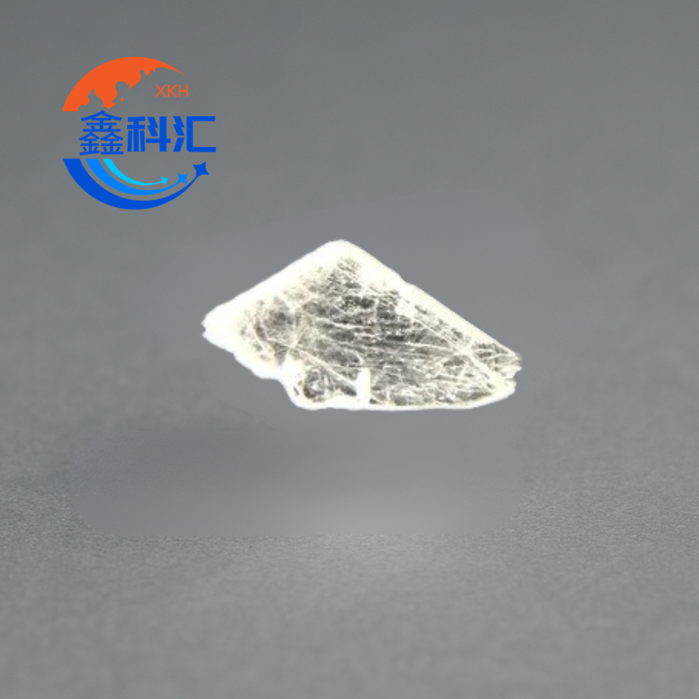
Graphene: A Powerful but Environment-Sensitive Material
Graphene is a single layer of carbon atoms arranged in a hexagonal lattice. It exhibits exceptional properties, including:
- Extremely high carrier mobility
- Excellent electrical conductivity
- High mechanical strength
- Atomic thickness
However, graphene’s biggest limitation is not its intrinsic performance, but its sensitivity to the environment.
When placed on conventional substrates such as silicon dioxide (SiO₂), graphene performance is significantly degraded due to:
- Surface roughness scattering
- Charged impurities at the interface
- Trap states and defects
- Chemical contamination
- Substrate-induced phonon scattering
These factors prevent graphene from reaching its theoretical electronic performance.
hBN: The Ideal 2D Insulating Partner
Hexagonal boron nitride (hBN) is a layered wide-bandgap material composed of boron and nitrogen atoms arranged in a graphene-like lattice.
Unlike typical dielectric materials, hBN offers a unique combination of properties:
- Atomically flat surface
- Strong chemical stability
- Wide bandgap (~6 eV)
- Extremely low charge impurity density
- Van der Waals surface compatibility
Most importantly, high-quality device-grade hBN single crystals provide an ultra-clean interface for graphene devices.
Why Graphene Needs hBN
The performance of graphene devices is not only determined by graphene itself, but by its interface environment. hBN solves many fundamental problems in graphene electronics:
1. Eliminating Surface Roughness Effects
hBN single crystals provide an atomically flat surface, minimizing electron scattering and preserving intrinsic graphene transport properties.
2. Reducing Charge Disorder
Compared to SiO₂, hBN has significantly fewer trapped charges, resulting in a much more uniform electrostatic environment for graphene.
3. Preserving Intrinsic Electronic Structure
Graphene interacts with hBN through weak van der Waals forces, avoiding strong chemical bonding that could distort its electronic bands.
4. Improving Device Stability
hBN protects graphene from environmental contamination, enhancing long-term device reliability.
The “hBN/Graphene/hBN” Sandwich Structure
One of the most important device architectures in modern 2D electronics is the fully encapsulated structure:
hBN / Graphene / hBN
This configuration provides:
- Ultra-clean interfaces above and below graphene
- Maximum reduction of disorder
- Enhanced carrier mobility
- Stable quantum transport behavior
- High reproducibility across devices
This structure is widely used in high-performance graphene research and quantum transport experiments.
Performance Enhancement Through hBN Single Crystals
When graphene is integrated with high-quality hBN single crystals, researchers observe:
- Dramatically increased carrier mobility
- Reduced charge inhomogeneity
- Strong quantum Hall effects
- Ballistic transport over longer distances
- Improved device-to-device consistency
In many cases, graphene mobility can increase by an order of magnitude compared to conventional substrates.
This demonstrates that substrate engineering is as important as graphene quality itself.
The Importance of Device-Grade hBN
Not all hBN materials deliver the same performance. The quality of the crystal directly affects graphene device behavior.
Device-grade hBN single crystals are characterized by:
- Large single-crystal domains
- Low defect density
- High dielectric breakdown strength
- Atomically smooth surfaces
- Minimal impurity concentration
These properties are essential for achieving reliable high-mobility graphene devices and reproducible research results.
Polycrystalline or lower-grade BN materials introduce disorder and significantly reduce device performance.
Beyond Electronics: Expanding Applications
The graphene–hBN combination is not limited to conventional electronics. It is also enabling new frontiers in:
- Quantum materials research
- Moiré superlattices and correlated electron systems
- Spin and valley physics
- Nanophotonics and polaritonics
- Next-generation quantum devices
In these systems, hBN is not just a passive substrate—it actively shapes the physical environment in which new quantum phenomena emerge.
Conclusion
Graphene and hBN form one of the most important material partnerships in modern science and engineering. While graphene provides extraordinary electronic capabilities, hBN single crystals provide the ideal environment to preserve and enhance those properties.
Together, they form the foundation of high-mobility graphene devices, van der Waals heterostructures, and emerging quantum technologies.
As research continues to push the boundaries of 2D electronics, the role of device-grade hBN single crystals will remain indispensable in unlocking the full potential of graphene-based systems.