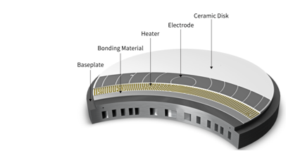
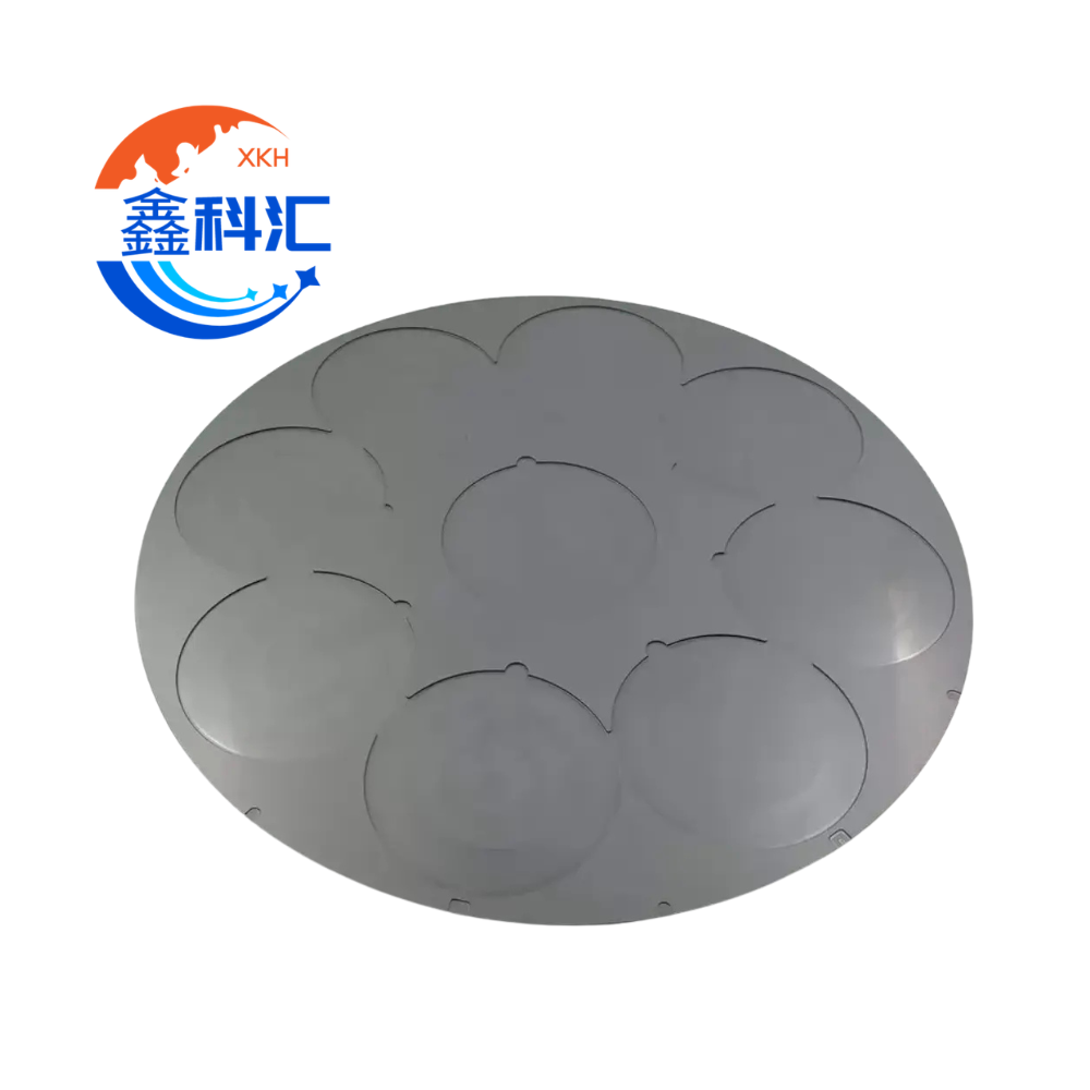
As 300mm wafers have become standard in advanced semiconductor manufacturing, wafer handling and process stability have become increasingly important. The electrostatic chuck, commonly known as an ESC, is one of the key components used to hold wafers securely during plasma etching, deposition, implantation, inspection and other semiconductor processes.
A 300mm electrostatic chuck uses electrostatic force to hold the wafer flat against the chuck surface without conventional mechanical clamping. This provides stable positioning while reducing physical contact with the wafer edge.
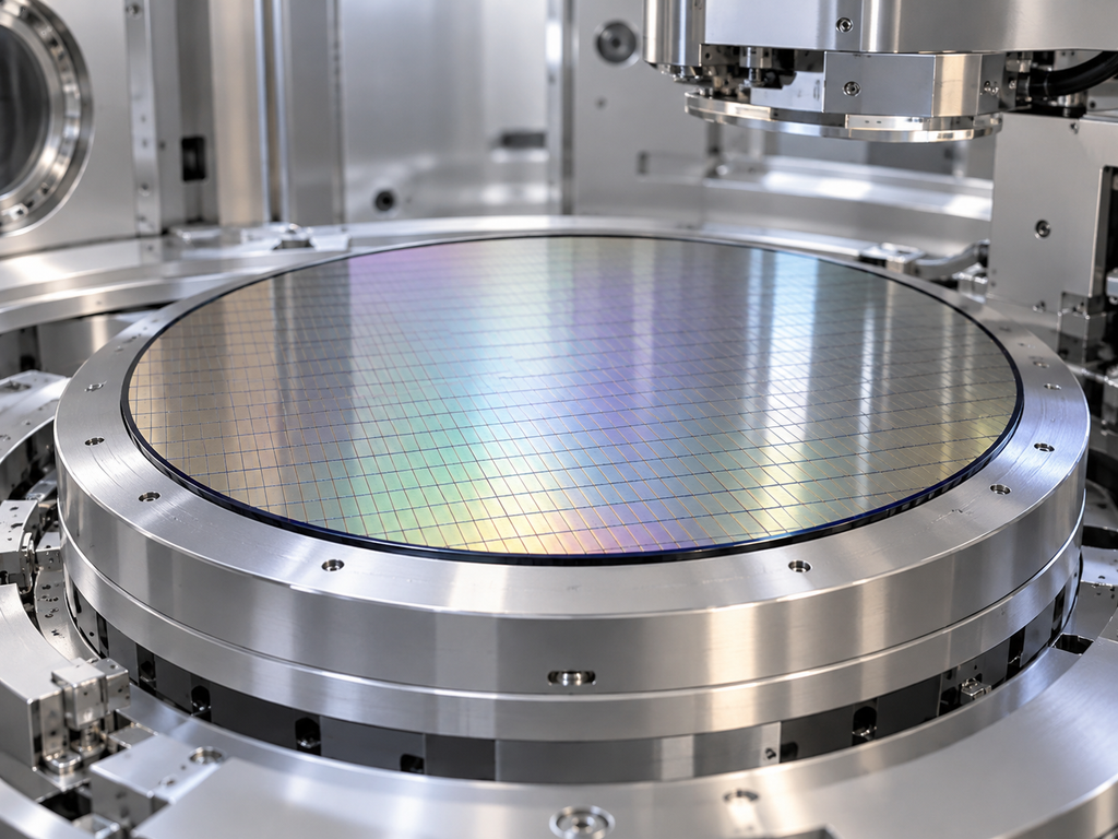
Why 300mm Wafer Holding Is More Challenging
Compared with smaller wafers, a 300mm wafer has a larger surface area and is more sensitive to local deformation, temperature variation and uneven clamping force.
If the holding force is not evenly distributed, several problems may occur:
- Local wafer bow or distortion
- Non-uniform thermal contact
- Process variation across the wafer
- Increased particle generation
- Reduced process repeatability
For this reason, the surface flatness, dielectric properties, electrode design and ceramic quality of the electrostatic chuck are critical.
Thermal Management
Temperature control is another major function of a semiconductor ESC.
During plasma etching and deposition, wafers may experience significant heat loads. The electrostatic chuck must provide stable thermal contact between the wafer and the temperature-controlled stage.
Many systems also use helium backside cooling to improve heat transfer between the wafer and the chuck surface. The design of backside gas grooves and sealing areas can strongly influence wafer temperature uniformity.
For advanced applications, both mechanical stability and thermal uniformity must be maintained over repeated heating and cooling cycles.
Yleiset keraamiset materiaalit
Several advanced ceramic materials are used for electrostatic chucks.
Alumina offers excellent electrical insulation, mature manufacturing processes and relatively good cost performance.
Aluminum nitride provides much higher thermal conductivity while maintaining electrical insulation, making it particularly suitable for applications requiring precise wafer temperature control.
Other ceramic and composite materials may also be selected depending on plasma resistance, electrical characteristics and process temperature.
Important Specifications
When selecting a 300mm electrostatic chuck, equipment manufacturers should consider:
- Wafer diameter
- Chuck surface flatness
- Electrostatic holding force
- Operating voltage
- Ceramic material
- Lämmönjohtavuus
- Pinnan karheus
- Backside helium cooling design
- Tyhjiöyhteensopivuus
- Plasman vastus
- Dimensional tolerance
- Long-term thermal stability
Custom ESC designs may also require specific electrode patterns, gas channels, lift pin holes or mounting interfaces.
Precision Manufacturing Matters
An electrostatic chuck is not simply a ceramic plate. It is a precision functional component that directly influences wafer stability and process consistency.
Large-diameter ESC manufacturing requires close control of ceramic sintering, precision grinding, electrode integration and surface finishing. Flatness and dimensional accuracy become increasingly difficult to maintain as the component size increases.
For semiconductor equipment manufacturers, working with a supplier experienced in advanced ceramic machining and customized wafer handling components can help reduce development risk.
As semiconductor manufacturing continues toward higher process precision and greater wafer productivity, the performance requirements for 300mm electrostatic chucks will continue to increase.