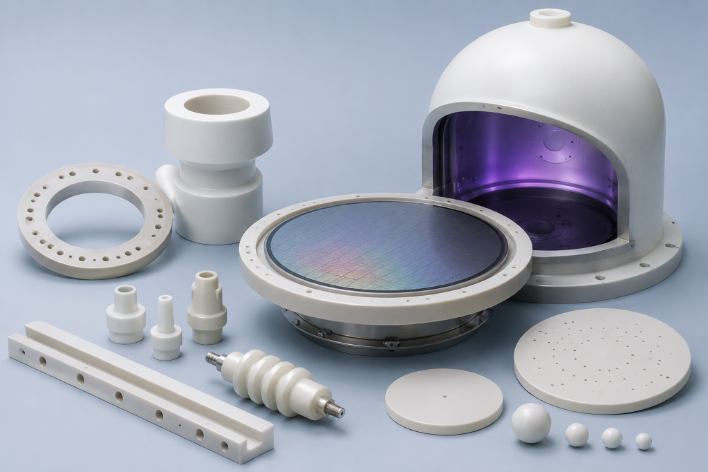
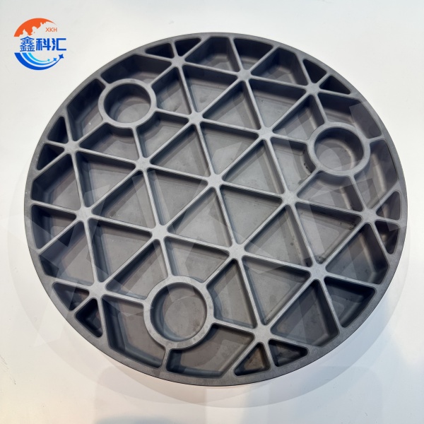
As semiconductor and optoelectronic technologies continue to advance toward higher power, greater integration, and improved reliability, the demand for high-performance materials is growing rapidly. Among the many advanced materials used in modern optoelectronic devices, ceramic materials have emerged as a critical enabling technology due to their exceptional thermal stability, chemical resistance, electrical insulation, and optical properties.
From semiconductor lasers and photovoltaic cells to optical sensors and advanced packaging, ceramic materials play an increasingly important role in improving device performance, extending operational lifetime, and enabling next-generation photonic technologies.
This article explores the key properties of ceramic materials, their applications in semiconductor optoelectronics, and future development trends shaping the industry.
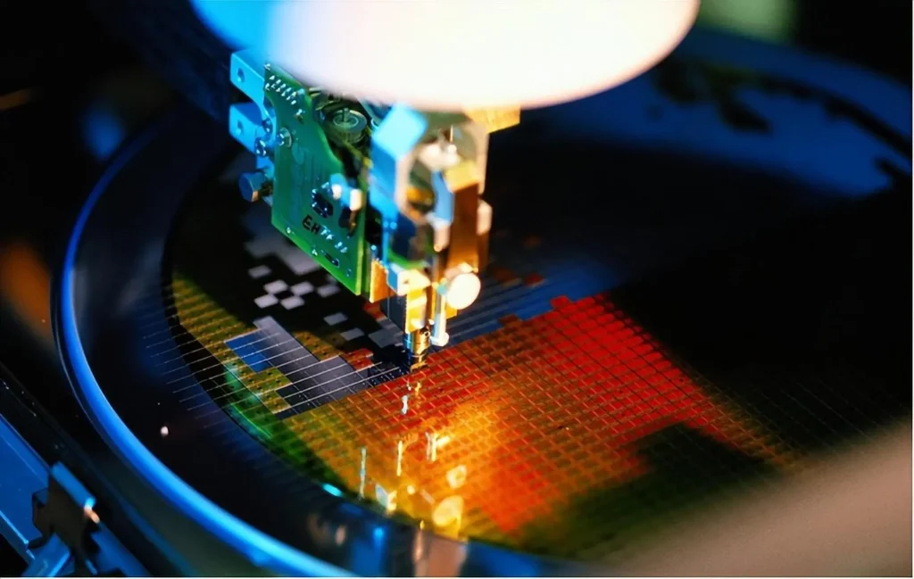
Why Ceramic Materials Matter in Semiconductor Optoelectronics
Semiconductor optoelectronic devices often operate under demanding conditions, including:
- Altas temperaturas
- Intense optical radiation
- Corrosive chemical environments
- High voltages and electric fields
- Frequent thermal cycling
Traditional materials may suffer from thermal deformation, corrosion, or performance degradation under such conditions. Advanced ceramics offer a unique combination of properties that help overcome these challenges.
Key Advantages of Ceramic Materials
Excelente estabilidad térmica
Many technical ceramics maintain their structural integrity and functional performance at temperatures exceeding 1000°C. This makes them suitable for high-power laser systems, semiconductor processing equipment, and harsh-environment sensors.
Resistencia química superior
Ceramics exhibit exceptional resistance to acids, alkalis, plasma environments, and reactive gases commonly used in semiconductor manufacturing processes.
High Electrical Insulation
Materials such as alumina and aluminum nitride provide excellent electrical insulation while maintaining thermal conductivity, making them ideal for electronic packaging and optoelectronic modules.
Outstanding Optical Properties
Certain advanced ceramics offer:
- High optical transparency
- Wide transmission windows
- Low optical absorption
- Excellent laser damage resistance
These characteristics are highly valuable for optical and photonic applications.
Resistencia mecánica y resistencia al desgaste
Ceramics possess high hardness and excellent dimensional stability, allowing long-term operation in demanding industrial environments.
Common Ceramic Materials Used in Optoelectronics
Alúmina (Al₂O₃)
Alumina is one of the most widely used engineering ceramics due to its:
- High insulation resistance
- Buena resistencia mecánica
- Excelente estabilidad química
- Cost-effectiveness
Las aplicaciones típicas son:
- Sustratos electrónicos
- Sensor components
- Envasado de LED
Nitruro de aluminio (AlN)
Combinaciones de nitruro de aluminio:
- Alta conductividad térmica
- Baja constante dieléctrica
- Excelente aislamiento eléctrico
Las aplicaciones incluyen:
- High-power LED packages
- Laser diode heat spreaders
- Dispositivos de RF y microondas
Nitruro de silicio (Si₃N₄)
Silicon nitride offers:
- Alta tenacidad a la fractura
- Excelente resistencia al choque térmico
- Resistencia superior al desgaste
Common uses include:
- Componentes de equipos semiconductores
- Rodamientos de precisión
- Structural optical parts
Carburo de silicio (SiC)
Silicon carbide ceramics provide:
- Conductividad térmica extremadamente alta
- Dureza excepcional
- Excelente resistencia a la corrosión
Las aplicaciones incluyen:
- Equipos de procesamiento de semiconductores
- Optical mirrors
- High-temperature optoelectronic systems
Cerámica transparente
Advanced transparent ceramics such as:
- YAG (Yttrium Aluminum Garnet)
- Spinel
- Alúmina transparente
are increasingly used in laser and photonic applications due to their optical transparency and mechanical durability.
Ceramic Materials in Semiconductor Laser Systems
Thermal Management of High-Power Lasers
Heat generation is one of the major limitations affecting semiconductor laser performance.
Ceramic materials with high thermal conductivity efficiently dissipate heat generated during operation, reducing:
- Thermal lensing effects
- Beam distortion
- Device degradation
Esto mejora:
- Output power stability
- Beam quality
- Device lifetime
Transparent Laser Ceramics
Transparent ceramics have become attractive alternatives to single crystals in solid-state laser systems.
Las ventajas incluyen:
- Large-scale manufacturing capability
- Uniform optical properties
- Lower production costs
- Flexible dopant distribution
YAG ceramic lasers are widely used in:
- Industrial cutting
- Medical treatment systems
- Defense applications
- Scientific research
Multi-Wavelength Laser Development
By engineering ceramic compositions and energy-level structures, researchers can develop laser materials capable of emitting multiple wavelengths.
These systems support applications such as:
- Optical communications
- Spectroscopy
- Biomedical imaging
- Precision manufacturing
Ceramic Materials in Photovoltaic Technology
As solar energy adoption accelerates worldwide, improving photovoltaic efficiency and durability remains a major focus.
Enhancing Conversion Efficiency
Advanced ceramic coatings and layers contribute to:
- Improved light absorption
- Reduced optical losses
- Enhanced charge transport
As a result, solar cells can achieve higher energy conversion efficiencies.
Protective Coatings
Ceramic coatings provide robust environmental protection against:
- UV radiation
- Moisture
- Temperature fluctuations
- Contaminación química
These protective layers significantly increase module reliability and operational lifespan.
Thermal Stability in Harsh Environments
Solar systems deployed in deserts, offshore installations, and industrial environments benefit from ceramic materials that maintain performance under extreme temperatures and harsh weather conditions.
Ceramic Materials in Optical Sensors
Optical sensors are widely used in:
- Medical diagnostics
- Environmental monitoring
- Industrial automation
- Aerospace systems
Ceramic materials have become important components in modern sensor design.
Improved Sensitivity
Specialized ceramic materials can be engineered to respond efficiently to specific wavelengths.
This enables:
- Higher signal detection accuracy
- Improved sensitivity
- Faster response times
Wider Detection Range
Transparent ceramic materials exhibit broad optical transmission windows, allowing sensors to detect radiation across:
- Ultraviolet (UV)
- Visible
- Near-infrared (NIR)
- Mid-infrared (MIR)
spectral regions.
Long-Term Reliability
Ceramic-based sensors maintain stable performance in environments characterized by:
- High humidity
- Gases corrosivos
- Altas temperaturas
- Radiation exposure
making them suitable for mission-critical applications.
Emerging Applications in Semiconductor Packaging
Advanced semiconductor packaging increasingly relies on ceramic materials for:
- Substrates
- Interpositores
- Dispersores de calor
- Hermetic packages
Particularly in:
- Electrónica de potencia
- Photonic integrated circuits (PICs)
- High-frequency communication modules
- AI computing hardware
materials such as aluminum nitride and silicon nitride provide excellent thermal and electrical performance.
Future Development Trends
Novel Ceramic Material Design
Researchers are developing advanced ceramic systems with:
- Tailored optical properties
- Mayor conductividad térmica
- Enhanced transparency
- Improved mechanical toughness
These materials are expected to unlock new optoelectronic device architectures.
Nanostructured Ceramics
Nanotechnology enables precise control over ceramic microstructures, leading to:
- Better optical performance
- Higher efficiency
- Reduced defects
- Improved device reliability
Multifunctional Integrated Devices
Future optoelectronic systems will increasingly require materials capable of simultaneously providing:
- Optical transmission
- Gestión térmica
- Aislamiento eléctrico
- Structural support
Advanced ceramics are uniquely positioned to meet these requirements.
Advanced Manufacturing Technologies
Emerging production methods such as:
- Additive manufacturing (3D printing)
- Spark plasma sintering (SPS)
- Precision ceramic machining
will enable more complex geometries and lower production costs.
Conclusión
Ceramic materials have become indispensable in modern semiconductor optoelectronics. Their exceptional thermal stability, corrosion resistance, electrical insulation, mechanical strength, and optical performance make them ideal for applications ranging from semiconductor lasers and photovoltaic cells to optical sensors and advanced packaging systems.
As material science continues to evolve, innovations in transparent ceramics, nanostructured materials, and multifunctional ceramic components are expected to drive the next generation of semiconductor and photonic technologies. With increasing demands for higher performance, reliability, and efficiency, advanced ceramic materials will remain a cornerstone of future optoelectronic innovation.