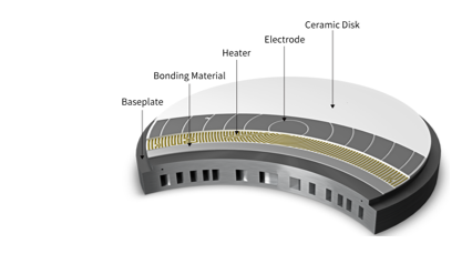
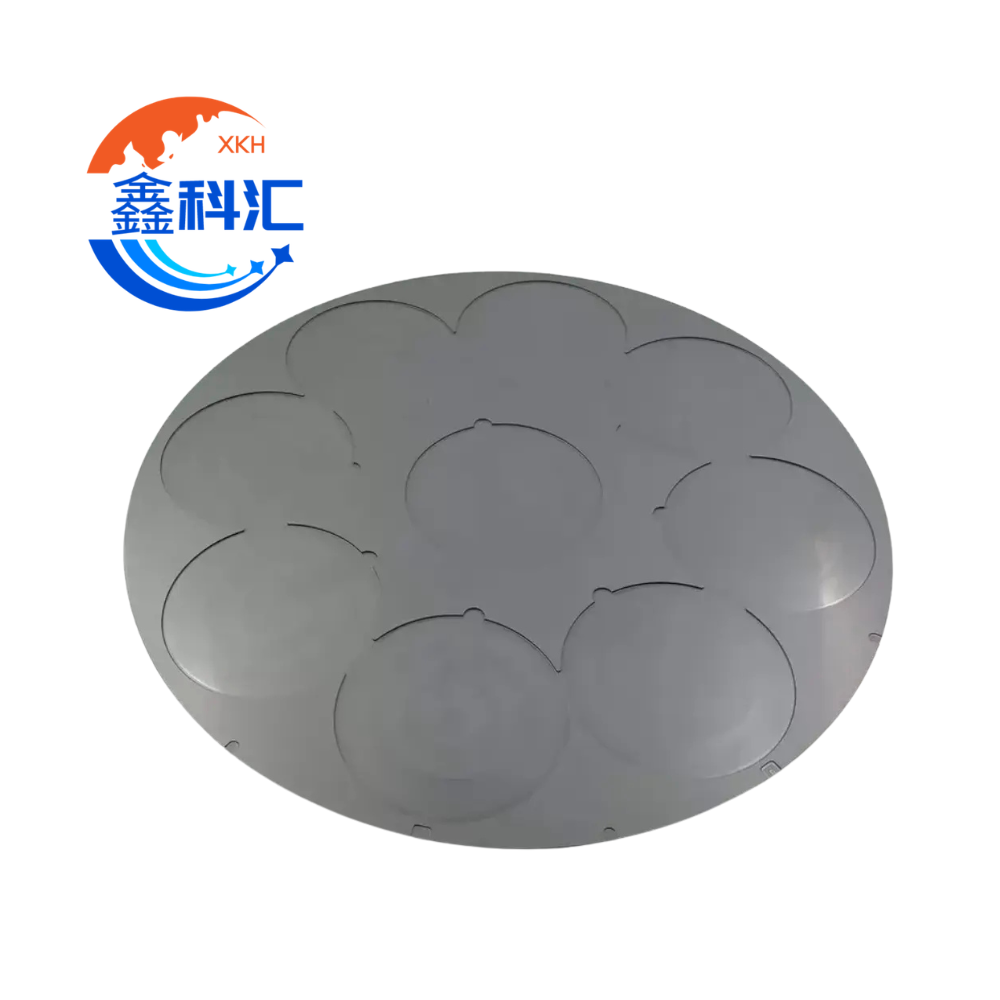
Precision ceramic rings are widely used in semiconductor manufacturing equipment where conventional metal components may struggle with
plasma exposure, electrical insulation, high temperature, corrosion, particle control or dimensional stability.
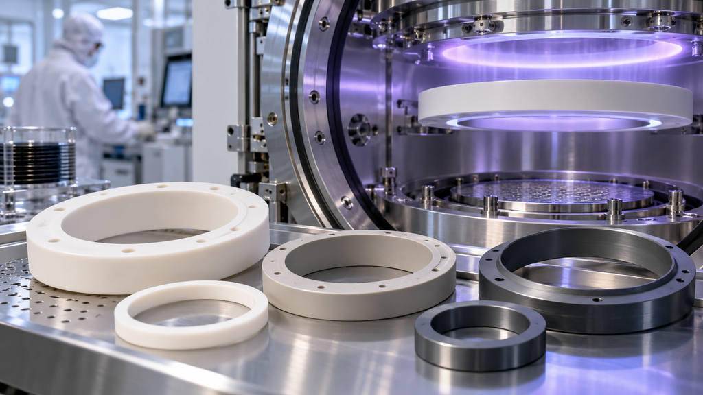
Depending on the equipment design, ceramic rings may function as focus rings, edge rings, chamber rings, insulating rings, support rings, sealing interfaces or structural components inside vacuum processing systems.
تشمل التطبيقات النموذجية ما يلي:
- معدات الحفر بالبلازما
- CVD and PECVD systems
- PVD and sputtering equipment
- أنظمة الزرع الأيوني
- Wafer heating and deposition equipment
- Vacuum process chambers
- Wafer handling assemblies
- Semiconductor inspection equipment
However, not every ceramic material performs equally well in every environment.
Among the most common engineering ceramics considered for semiconductor equipment are alumina (Al₂O₃), aluminum nitride (AlN) and silicon carbide (SiC).
Material selection should consider much more than mechanical strength. Plasma chemistry, temperature, thermal conductivity, electrical behavior, purity, dimensional tolerance and surface finish may all determine the final performance of a ceramic ring.
1. Why Are Ceramic Rings Used in Semiconductor Equipment?
Many semiconductor processes take place inside environments involving:
- High vacuum
- Reactive gases
- RF or microwave plasma
- Elevated temperatures
- التدوير الحراري السريع
- High electrical fields
- Strict particle-control requirements
Components located close to the wafer may directly influence process stability and wafer yield.
In plasma etch systems, for example, focus or edge rings are positioned around the wafer perimeter to help control plasma behavior near the wafer edge and improve etch uniformity. Ceramic components used in these chambers must withstand reactive process gases, plasma exposure and repeated cleaning cycles.
Ceramics are attractive because they can provide combinations of:
- العزل الكهربائي
- صلابة عالية
- الثبات الحراري
- مقاومة التآكل
- مقاومة المواد الكيميائية
- توليد جسيمات منخفضة
- Precision-machined surfaces
- High-purity material options
The correct ceramic, however, depends strongly on the actual process.
2. Alumina Ceramic Rings
Alumina, or aluminum oxide, is one of the most widely used technical ceramic materials.
For semiconductor applications, high-purity grades are usually preferred because purity can influence contamination, corrosion behavior and performance in demanding process environments.
Advantages of Alumina
Alumina ceramic offers:
- High electrical insulation
- Good dielectric strength
- صلابة عالية
- مقاومة جيدة للتآكل
- مقاومة جيدة للمواد الكيميائية
- ثبات أبعاد جيد
- Mature manufacturing technology
- Competitive cost compared with many specialty ceramics
High-purity alumina is already widely used for semiconductor plasma equipment components such as focus rings, nozzles, liners, windows and other chamber parts.
التطبيقات النموذجية
Alumina rings may be suitable for:
- الحلقات العازلة
- Chamber support rings
- Focus-ring structures
- Vacuum insulation components
- Wafer handling assemblies
- Electrical isolation components
- Deposition chamber rings
Alumina is often a practical starting point where electrical insulation, mechanical stability and cost need to be balanced.
Purity Considerations
Alumina is available in many purity levels.
For general industrial ceramic parts, lower-purity grades may be sufficient. Semiconductor applications, however, frequently require high-purity or ultra-high-purity compositions.
Higher alumina purity generally improves resistance to contamination and can improve performance in aggressive process environments.
For critical semiconductor chamber components, material purity should therefore be defined in the drawing or purchase specification rather than simply specifying “Alumina.”
3. Aluminum Nitride Ceramic Rings
Aluminum nitride, commonly abbreviated as AlN, occupies a different position from alumina.
Its most important characteristic is the combination of high thermal conductivity and electrical insulation.
This makes AlN especially valuable when heat must be transferred efficiently without creating an electrically conductive path. Semiconductor equipment manufacturers commonly use AlN in heaters and other thermal-management components for this reason.
Advantages of AlN
AlN provides:
- موصلية حرارية عالية
- عزل كهربائي ممتاز
- Relatively low thermal expansion
- Good high-temperature capability
- ثبات أبعاد جيد
- Suitable properties for thermal management
التطبيقات النموذجية
AlN ceramic rings may be considered for:
- Heater assemblies
- Wafer-heating structures
- Temperature-control components
- Electrically insulating thermal interfaces
- Semiconductor process chamber components
- Ring structures close to heated wafer stages
When a ceramic ring is located close to a heater, hot wafer or temperature-controlled stage, thermal gradients can become important.
A material with higher thermal conductivity can help distribute heat more effectively and reduce local temperature differences.
For this reason, AlN may offer advantages over alumina when thermal management is a primary design requirement.
4. Silicon Carbide Ceramic Rings
Silicon carbide is widely used in semiconductor equipment where high stiffness, wear resistance, dimensional stability and thermal performance are required.
Depending on manufacturing route, semiconductor equipment may use different forms of SiC, including sintered SiC, reaction-bonded SiC, recrystallized SiC and high-purity CVD SiC.
These materials should not automatically be treated as interchangeable.
Advantages of SiC
ومن المزايا النموذجية ما يلي:
- صلابة عالية
- Excellent stiffness
- موصلية حرارية عالية
- تمدد حراري منخفض
- مقاومة جيدة للتآكل
- High-temperature capability
- ثبات أبعاد جيد
- Availability in high-purity grades
SiC is used in semiconductor equipment for chamber components, wafer-handling parts, vacuum chucks, electrostatic chuck-related structures and chamber rings.
When SiC Is Preferred
SiC may be particularly attractive when the ring requires:
- High structural rigidity
- مقاومة التشوه
- Low thermal distortion
- Rapid heat transfer
- High-temperature operation
- ثبات الأبعاد على المدى الطويل
For large-diameter ring structures, stiffness and thermal expansion can become increasingly important because even relatively small dimensional changes may influence wafer alignment or chamber geometry.
5. Plasma Applications: Material Selection Requires More Than Hardness
Plasma processing environments are among the most demanding applications for semiconductor ceramic parts.
During etching or deposition, ceramic components may be exposed to:
- Fluorine-containing plasma
- Chlorine-containing chemistry
- Oxygen plasma
- Reactive radicals
- Ion bombardment
- RF energy
- Repeated plasma cleaning
Material erosion can gradually change component dimensions and may also create particles.
For this reason, plasma compatibility cannot be evaluated only from bulk hardness.
Important factors include:
- Plasma chemistry
- Plasma power
- Chamber pressure
- Component temperature
- Ion energy
- Material purity
- Grain structure
- Surface condition
- Coating condition
For particularly aggressive etch applications, materials such as high-purity alumina, SiC, yttria and specialized coatings may be considered depending on the chamber location and chemistry. Commercial semiconductor component suppliers offer these different ceramic families specifically because no single material is optimum for every plasma environment.
6. Ceramic Rings in Vacuum Environments
Vacuum compatibility is another major consideration.
Semiconductor ceramic components may operate under high vacuum or controlled low-pressure process conditions.
A suitable ceramic ring should maintain:
- ثبات الأبعاد
- تلوث منخفض
- Stable mechanical properties
- Reliable interfaces with adjacent components
- Clean surface conditions
Ceramic components are commonly used in vacuum process equipment because they can combine electrical insulation, thermal resistance and chemical stability without many of the limitations associated with polymers.
However, the ceramic itself is only part of the design.
Blind holes, trapped volumes, adhesives, surface contamination and assembly interfaces can all influence vacuum performance.
The complete component design should therefore be evaluated rather than considering only the ceramic material.
7. Thermal Expansion and Dimensional Stability
A ceramic ring does not operate independently.
It may be assembled with:
- Aluminum
- Stainless steel
- Titanium
- كوارتز
- Graphite
- Silicon
- Other ceramic materials
These materials expand at different rates when temperature changes.
If a ceramic ring is rigidly constrained by a metal holder, thermal expansion mismatch may generate mechanical stress.
This may lead to:
- Ring cracking
- Distortion
- Loss of concentricity
- Changes in gap dimensions
- Surface contact problems
Therefore, engineers should consider both ceramic properties and the surrounding assembly.
For temperature-sensitive systems, SiC and AlN may provide advantages where thermal stability or thermal transfer is particularly important.
8. Dimensional Tolerance of Precision Ceramic Rings
Semiconductor equipment often requires ceramic rings with significantly tighter tolerances than ordinary industrial ceramic components.
Important specifications may include:
Outer Diameter
The OD may interface with a chamber, holder or positioning structure.
Inner Diameter
The ID may define clearance around a wafer, electrode or other processing component.
Concentricity
Good concentricity is particularly important for rings positioned around wafers or rotating assemblies.
Flatness
Poor flatness may create uneven contact or affect assembly positioning.
Parallelism
The two major faces may need to remain closely parallel.
Thickness
Thickness can influence chamber gaps, wafer position and process geometry.
Roundness
Large ceramic rings may require careful control of circular geometry after sintering and final grinding.
The appropriate tolerance should be determined according to ring size, wall thickness, ceramic material and equipment function.
9. Surface Roughness and Surface Condition
Surface finish is particularly important for components used close to semiconductor wafers.
A precision-machined ceramic surface may reduce particle generation and provide more repeatable contact.
Depending on the application, processes may include:
- الطحن الدقيق
- Fine grinding
- Lapping
- التلميع
- Edge finishing
Ra requirements should be selected according to function.
A mounting surface, plasma-exposed surface and wafer-contact surface may require different surface finishes.
Extremely low Ra should not automatically be specified on every surface because additional polishing increases manufacturing complexity and cost without necessarily improving equipment performance.
10. Edge Chipping and Chamfer Design
Technical ceramics are hard but brittle.
Sharp corners are particularly vulnerable during:
- Machining
- التنظيف
- Transportation
- Installation
- Equipment maintenance
Precision ceramic rings should therefore normally include controlled chamfers or radii where permitted by the design.
Common drawing requirements may specify:
- Edge chamfer
- Maximum allowable chip size
- Cosmetic defect criteria
- Crack restrictions
For thin ceramic rings, edge design becomes even more important because the available cross-section is limited.
11. Large-Diameter Ceramic Rings
As semiconductor wafers have moved toward 200 mm and 300 mm platforms, ceramic components around the wafer have also become larger.
Producing large ceramic rings presents additional challenges.
These include:
- Sintering shrinkage
- Warpage
- Flatness control
- Diameter tolerance
- Concentricity
- Grinding stress
- Handling damage
Large-diameter rings usually require sufficient machining allowance after sintering so that final geometry can be established through precision grinding.
Material selection also becomes more significant because stiffness and thermal expansion influence performance over a larger diameter.
12. Alumina vs. AlN vs. SiC
There is no universally best ceramic material.
A simplified selection approach is:
Choose Alumina When:
- Electrical insulation is important
- Good wear resistance is required
- High-purity ceramic is needed
- Cost sensitivity matters
- The thermal-management requirement is moderate
Choose AlN When:
- High thermal conductivity is important
- Electrical insulation must also be maintained
- The ring is located near a heater or thermal stage
- Temperature uniformity is important
Choose SiC When:
- High stiffness is required
- Thermal expansion must be minimized
- High thermal conductivity is useful
- Wear resistance is important
- The component operates in demanding semiconductor equipment
Actual material selection should still be confirmed according to plasma chemistry, chamber temperature, electrical requirements and contamination limits.
13. Information Required for Custom Ceramic Rings
For custom semiconductor ceramic ring projects, customers should ideally provide a 2D drawing or 3D CAD model.
Important RFQ information includes:
- Material: Al₂O₃ / AlN / SiC
- Material purity
- Outer diameter
- Inner diameter
- Thickness
- Flatness
- Parallelism
- Concentricity
- Dimensional tolerances
- خشونة السطح
- Chamfer or radius requirements
- Hole quantity and dimensions
- Groove geometry
- درجة حرارة التشغيل
- Vacuum level
- Plasma chemistry
- المتطلبات الكهربائية
- Cleaning requirements
- الكمية
The intended application should also be described whenever possible.
على سبيل المثال:
Plasma etch focus ring
و
vacuum chamber insulating ring
may have similar geometry but completely different material requirements.
14. Custom Precision Ceramic Rings from XKH Ceramics
Precision ceramic rings for semiconductor equipment require careful coordination between material properties, component geometry and process conditions.
Alumina provides an excellent combination of electrical insulation, hardness, chemical resistance and manufacturing maturity.
Aluminum nitride is particularly valuable where heat must be transferred efficiently while maintaining electrical insulation.
Silicon carbide provides excellent rigidity, thermal stability, wear resistance and dimensional performance for demanding equipment structures.
XKH Ceramics provides custom precision ceramic components for semiconductor equipment based on customer drawings and application requirements.
Available ceramic solutions include:
- High-purity alumina ceramic parts
- Aluminum nitride components
- Silicon carbide ceramic components
- Ceramic rings
- Focus-ring structures
- Ceramic plates
- Insulating components
- Precision-machined ceramic parts
For a new semiconductor ceramic ring project, providing the material, dimensions, tolerance, surface roughness, operating environment and application allows manufacturing feasibility and the appropriate material solution to be evaluated more accurately.