As plasma etch, PECVD, CVD and other semiconductor processes move toward tighter temperature windows and higher plasma power, the electrostatic chuck has become much more than a wafer-holding component.
For 300mm semiconductor equipment, the ceramic electrostatic chuck, or ESC, simultaneously affects wafer clamping, backside helium cooling, RF power delivery, wafer temperature uniformity, particle performance and process repeatability.
A poorly matched ESC can cause problems such as local temperature variation, unstable helium pressure, backside particles, wafer sticking, dechuck failure, RF arcing or non-uniform plasma behavior.
For equipment manufacturers and replacement-part buyers, selecting an ESC therefore requires more than specifying only the wafer diameter and ceramic material.
The ceramic composition, electrode structure, gas channels, surface geometry, flatness and integration with the cooling base must all be considered together.
What Does a 300mm Electrostatic Chuck Do?
An electrostatic chuck uses an electric field to hold a semiconductor wafer against a ceramic surface without relying on conventional mechanical clamps.
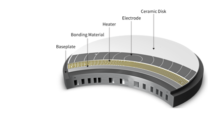
Inside the ceramic body, one or more conductive electrodes are embedded beneath the wafer-supporting surface.
When voltage is applied, electrostatic attraction holds the wafer in position.
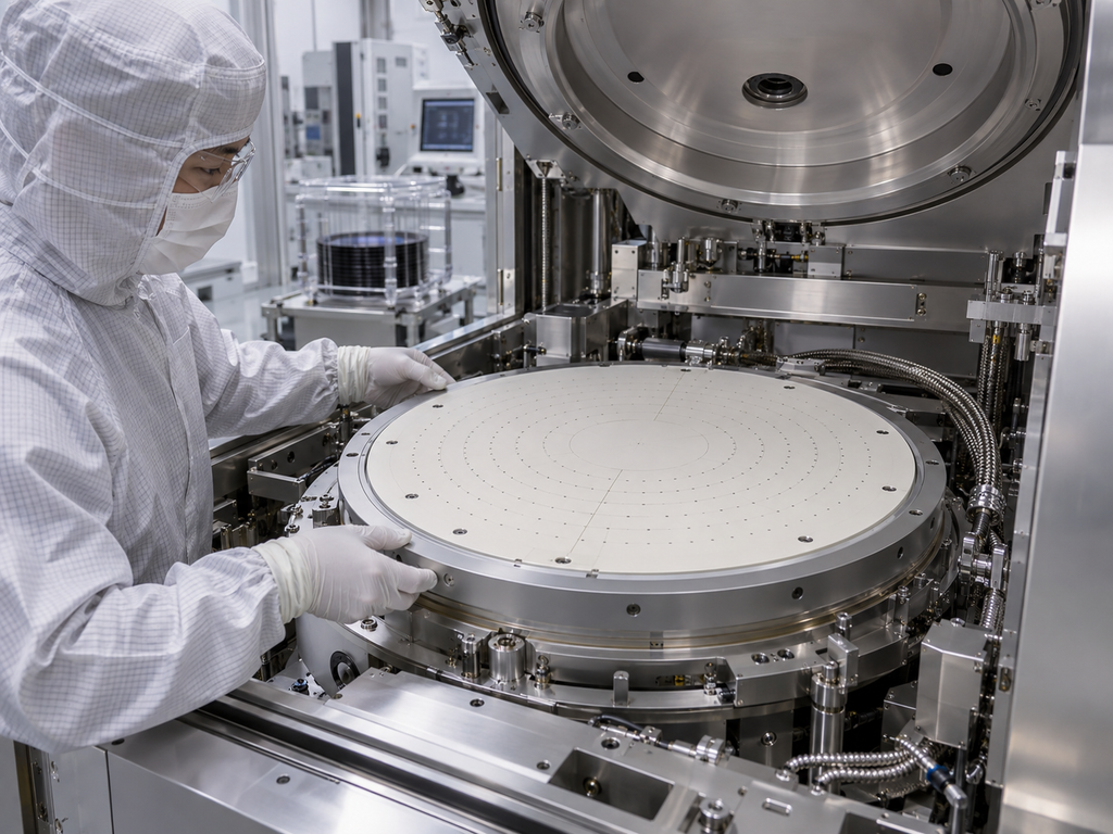
In many etch and deposition systems, the ESC is installed above a temperature-controlled metal base. Helium is introduced between the wafer backside and the ceramic surface to improve heat transfer.
This creates several functions in one assembly:
wafer clamping, wafer positioning, thermal management, RF interaction, backside gas distribution and mechanical support.
These functions are strongly coupled.
For example, a change in surface flatness can alter the local helium gap. That can change thermal conductance, which changes wafer temperature and may ultimately affect etch rate or film properties.
For this reason, an ESC should be treated as a precision process component rather than simply a ceramic plate.
AlN vs Alumina for Semiconductor ESCs
Aluminum nitride and alumina are two important ceramic materials used in electrostatic chuck structures.
Neither material is universally superior.
The correct choice depends on process temperature, plasma conditions, thermal load, electrical design, purity requirements and cost targets.
| الممتلكات | سيراميك AlN | سيراميك الألومينا |
|---|---|---|
| التوصيل الحراري | عالية | معتدل |
| العزل الكهربائي | Excellent when properly controlled | ممتاز |
| Thermal response | Fast | Slower |
| Temperature uniformity potential | Very good | جيد |
| High-temperature capability | ممتاز | ممتاز |
| Mechanical stability | عالية | عالية |
| Material/process cost | أعلى | Generally lower |
| Typical attraction | High thermal-load ESCs | Mature, cost-effective ESC designs |
Why AlN Is Often Selected
The strongest advantage of aluminum nitride is its high thermal conductivity.
Compared with conventional alumina ceramics, AlN can transport heat through the ceramic body much more efficiently.
This becomes important when the wafer is exposed to high plasma power or when the process requires tight wafer-temperature uniformity.
For a 300mm wafer, even a relatively small center-to-edge temperature difference can affect process results.
AlN therefore becomes attractive for applications involving high plasma density, rapid thermal response, narrow process windows or integrated heater structures.
AlN also has a relatively low coefficient of thermal expansion compared with many other technical ceramics, which can be useful when controlling dimensional stability across repeated thermal cycles.
However, AlN ESC performance depends strongly on ceramic purity, sintering additives, electrical resistivity and electrode integration.
The term “AlN ESC” alone is therefore not a sufficient technical specification.
Why Alumina Is Still Widely Used
Alumina remains attractive because it is a highly mature semiconductor ceramic.
High-purity alumina provides good electrical insulation, mechanical strength, dimensional stability and manufacturing repeatability.
It is also generally more economical than high-performance AlN.
For processes where heat flux is moderate and extreme thermal conductivity is not required, alumina can provide a very practical ESC solution.
However, formulations containing additives must be carefully controlled.
Ceramic composition affects electrical behavior, plasma compatibility and contamination performance.
For semiconductor applications, the supplier should therefore distinguish between ordinary industrial alumina and semiconductor-grade ceramic material.
Coulombic and Johnsen-Rahbek ESC Behavior
Ceramic material selection also interacts with the electrostatic clamping mechanism.
ESCs are commonly associated with Coulombic or Johnsen-Rahbek-type behavior.
A highly insulating dielectric tends to support Coulombic clamping, where electrostatic attraction is generated across the dielectric.
Johnsen-Rahbek behavior involves controlled electrical conduction at the interface and can produce stronger clamping forces at lower applied voltages under certain conditions.
The ceramic resistivity therefore becomes an important design variable.
It is not sufficient to specify only:
“AlN, 99% purity”
or
“Alumina ceramic.”
Electrical resistivity, operating temperature and intended clamping mechanism may also need to be defined.
This is especially important because ceramic resistivity can vary significantly with temperature.
An ESC that performs correctly at room temperature may behave differently at an elevated process temperature.
Why Helium Backside Cooling Is Required
In a vacuum chamber, heat transfer between the wafer and ESC surface is limited because there is very little gas between them.
Direct solid-to-solid contact exists only at limited microscopic contact points.
During plasma processing, however, the wafer may receive significant thermal energy.
Backside helium is therefore introduced into the small space between the wafer and the ESC.
Helium has good thermal conductivity and creates a much more effective thermal path between the wafer and the temperature-controlled chuck.
The general thermal path becomes:
Wafer → Backside He → Ceramic ESC → Bond/interface → Cooling base → Chiller
If one part of this chain is unstable, wafer temperature uniformity can deteriorate.
Helium Groove and Hole Design
Backside gas is normally distributed through holes and surface channels or grooves.
For 300mm ESCs, the design must achieve sufficiently uniform pressure beneath the wafer without causing excessive leakage or introducing electrical discharge risk.
Important parameters include helium-hole position, hole diameter, channel depth, groove pattern, edge seal geometry, surface roughness and wafer contact area.
The system may also use separate helium zones.
For example, the center and edge of the wafer can be controlled independently.
This makes it possible to compensate for radial thermal differences.
A multi-zone ESC can therefore provide greater thermal tuning capability than a simple single-pressure design.
However, more zones also increase manufacturing and integration complexity.
Helium Leakage Is an Important Diagnostic Parameter
Stable He pressure depends on the condition of the wafer, chuck surface and sealing region.
Unexpectedly high helium flow may indicate several possible issues.
These can include wafer bow, particles beneath the wafer, damage to the edge seal area, poor ESC flatness, surface wear or contamination.
Therefore, backside helium flow and pressure can sometimes provide useful information about the mechanical condition of the ESC.
A sudden change in He behavior should not automatically be treated as a gas-system problem.
The ESC surface itself should also be inspected.
RF Coupling Creates Additional ESC Design Challenges
In many plasma etch systems, the wafer stage does more than clamp and cool the wafer.
It may also participate in RF bias delivery.
This makes the ESC an electrical as well as a thermal component.
RF energy can interact with embedded electrodes, the metal base, helium channels and nearby dielectric regions.
At higher RF voltages and power levels, unwanted electric fields around gas holes or internal interfaces can increase the risk of arcing.
Published ESC designs therefore use measures such as ceramic sleeves, porous ceramic plugs and modified gas paths to reduce direct electrical paths through helium openings.
Porous AlN or alumina structures can allow backside gas flow while helping suppress plasma penetration or electrical breakdown inside the gas channel.
This becomes increasingly important as plasma tools operate at higher bias power.
Helium Hole Arcing and Ignition
A helium supply hole may appear mechanically simple, but electrically it can become a critical feature.
The combination of RF voltage, pressure, geometry and conductive surfaces may allow a discharge to form inside the gas pathway.
Potential consequences include local arcing, surface damage, particle generation, wafer-backside contamination and premature ESC failure.
For this reason, He-hole design may incorporate a non-line-of-sight path, insulating ceramic features or porous ceramic inserts.
The goal is to maintain sufficient helium conductance while reducing the possibility of electrical breakdown.
The exact design must be matched to the chamber’s RF voltage, operating pressure and gas-flow requirements.
Flatness Matters More Than the Diameter Suggests
A 300mm wafer covers a large surface area.
Small local height differences across the ESC therefore matter.
If the ESC mounting surface is not sufficiently flat, contact between the wafer and ceramic becomes nonuniform.
This can change local backside helium gaps.
The result may be different thermal conductance in different wafer regions.
In high-sensitivity processes, these temperature differences can translate into differences in etch rate, critical dimension, deposition rate or film properties.
Flatness should therefore be evaluated together with surface geometry rather than as an isolated drawing tolerance.
Important geometric characteristics may include total flatness, local flatness, parallelism, ceramic thickness variation, baseplate flatness, bond-layer uniformity and edge-zone geometry.
ESC Warpage Can Change During Temperature Cycling
Flatness measured at room temperature does not always represent the operating condition.
An ESC assembly may contain several materials:
ceramic, embedded metal electrodes, brazed or bonded interfaces, aluminum cooling bases and heater structures.
These materials have different thermal expansion behavior.
As the chuck heats or cools, internal stress can change the surface profile.
For high-temperature CVD or plasma processes, it can therefore be important to evaluate thermal deformation as well as room-temperature geometry.
Material matching and bonding design become particularly important in large 300mm assemblies.
Surface Roughness and Mesa Design
The wafer usually does not contact the entire ESC surface.
Many ESC designs use raised contact areas, often referred to as mesas or bumps.
Reducing the real contact area can help control friction, backside contamination and dechucking behavior.
However, the surface geometry must be carefully manufactured.
If mesas are too high, too low or nonuniform, wafer support and helium distribution may be affected.
If the surface is too rough, particles can be trapped or generated.
If it is excessively smooth, adhesion and dechucking behavior can also change.
Therefore, surface finish should be treated as a functional parameter rather than a cosmetic specification.
Particle Control Starts at the Wafer Contact Surface
Particle control is one of the most important ESC quality requirements.
Potential particle sources include ceramic surface defects, machining residue, polishing debris, damaged mesas, contaminated helium holes, coating failure, bond-interface damage and wafer-contact wear.
Particle problems can become especially difficult because the ESC may remain mechanically functional while gradually contaminating wafers.
For this reason, semiconductor ESC manufacturing requires strong control of machining, polishing, cleaning and packaging.
Final cleaning procedures should match the customer’s contamination requirements.
After cleaning, ceramic components should be handled and packaged in a controlled environment to reduce recontamination before installation.
Purity Alone Does Not Guarantee Low Contamination
It is common for buyers to ask only for “high-purity AlN” or “high-purity alumina.”
Purity is important, but contamination performance also depends on secondary phases, sintering additives, machining consumables, cleaning chemistry and handling.
A nominally high-purity ceramic can still produce unacceptable contamination if the manufacturing process is poorly controlled.
For semiconductor ESC applications, supplier qualification should therefore consider both raw material and finished-component processing.
Critical Features for a Custom 300mm ESC
When requesting a custom or replacement ESC, the engineering discussion should cover the full assembly.
Useful RFQ information includes the following:
- wafer diameter and wafer type;
- Etch, PECVD, CVD or other process;
- ESC ceramic material;
- ceramic purity or composition requirement;
- Coulombic or Johnsen-Rahbek design;
- monopolar or bipolar electrode structure;
- operating voltage;
- operating temperature;
- RF frequency and RF power;
- backside helium pressure and flow requirement;
- number of He cooling zones;
- helium-hole and groove drawing;
- surface flatness and parallelism;
- surface roughness;
- mesa/contact pattern;
- electrode material and position;
- heater requirement;
- metal cooling-base dimensions;
- cooling-channel structure;
- bonding or brazing requirement;
- backside interface;
- particle and contamination limits;
- drawing, STEP model or reference sample.
Providing this information allows the ceramic manufacturer to determine whether an existing structure can be reproduced or whether the ESC requires redesign.
AlN or Alumina: Which One Should You Specify?
The choice should begin with the process rather than with the material name.
For high thermal-load processes where rapid heat spreading and tight wafer-temperature control are major priorities, AlN is often attractive.
For mature processes with moderate thermal demands, alumina can provide a strong combination of electrical insulation, manufacturing maturity and cost efficiency.
But ceramic selection cannot be separated from the complete ESC architecture.
An AlN plate with poor flatness, unstable electrical properties or poorly designed helium channels may perform worse than a properly engineered alumina ESC.
Likewise, replacing an alumina component with AlN without considering RF, thermal expansion and electrode design is not automatically an upgrade.
The correct engineering question is therefore not simply:
“AlN or Alumina?”
It is:
“Which ceramic and ESC structure provides the required electrical, thermal and contamination performance for this specific 300mm process?”
Replacement ESC and Reverse Engineering
In semiconductor equipment maintenance, replacement ESC projects do not always begin with complete OEM drawings.
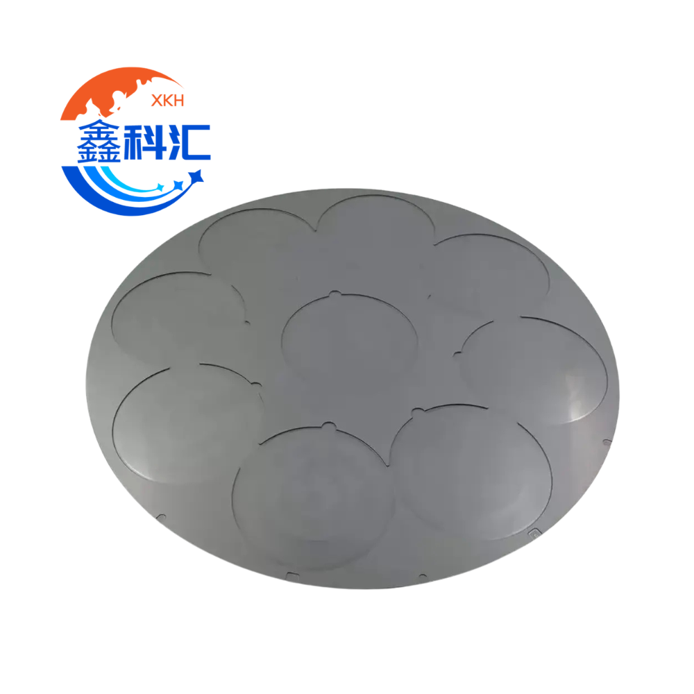
In some cases, customers provide a used ESC or ceramic puck for dimensional analysis.
Reverse engineering may include measurement of overall diameter, thickness, hole locations, gas-channel geometry, electrode position, surface pattern, interface dimensions and mounting features.
However, used components must be evaluated carefully.
Wear, erosion, deposits and thermal deformation can cause the measured geometry to differ from the original design.
Where possible, the sample should be combined with equipment information, process conditions and previous inspection data.
This reduces the risk of reproducing an already worn geometry.
الخاتمة
A 300mm ceramic electrostatic chuck is a tightly integrated thermal, electrical and mechanical subsystem.
Its performance depends on much more than ceramic purity or wafer diameter.
AlN offers strong thermal conductivity and is attractive for high heat-flux processes, while alumina remains a mature and cost-effective option for many plasma applications.
Backside helium improves wafer cooling, but gas-channel geometry, edge sealing and surface flatness determine how uniformly that cooling reaches the wafer.
At the same time, RF coupling introduces additional challenges around helium holes, embedded electrodes and dielectric interfaces.
As plasma power and process requirements increase, arcing prevention and electrical isolation become increasingly important.
For semiconductor equipment manufacturers and replacement-part buyers, the most effective ESC specification combines:
ceramic material + electrical properties + electrode design + thermal design + helium distribution + flatness + surface structure + contamination control.
When these parameters are engineered together, the ESC can provide stable wafer clamping, repeatable temperature control, lower particle risk and longer service life in demanding 300mm etch and CVD processes.
الأسئلة الشائعة
Is AlN always better than alumina for a 300mm electrostatic chuck?
No. AlN provides significantly better thermal conductivity, which can benefit high heat-load processes, but alumina remains suitable for many ESC applications because of its insulation performance, manufacturing maturity and lower cost. The correct choice depends on temperature, RF conditions, electrical design and contamination requirements.
Why is helium used behind the wafer on an electrostatic chuck?
Vacuum provides poor heat transfer between the wafer and the chuck. Helium introduced between the wafer backside and ESC surface improves thermal conduction, allowing heat to move more efficiently from the wafer to the temperature-controlled chuck.
Why can helium holes cause RF arcing?
The helium pathway contains gas close to electrically active parts of the ESC. Under certain combinations of RF voltage, pressure and geometry, electrical discharge can occur. Ceramic sleeves, porous AlN or alumina plugs and optimized gas-hole geometry can be used to reduce this risk.
How does ESC flatness affect the semiconductor process?
Poor flatness changes the gap and contact condition between the wafer and ESC. This can cause nonuniform helium heat transfer and therefore wafer-temperature variation, potentially affecting etch or deposition uniformity.
What information is needed to quote a custom 300mm ESC?
The most useful information includes wafer size, ceramic material, process type, operating temperature, RF conditions, ESC voltage, He cooling structure, electrode configuration, flatness, surface finish, cooling-base design and an engineering drawing or reference sample.