The rapid expansion of two-dimensional (2D) materials research has opened entirely new directions in electronics, photonics, and quantum technologies. Materials such as graphene, transition metal dichalcogenides (TMDs), and other atomically thin crystals exhibit extraordinary properties that differ fundamentally from their bulk counterparts.
However, the practical realization of high-performance 2D devices depends not only on the active material itself, but also critically on the surrounding environment. In this context, hexagonal boron nitride (hBN) single crystals have emerged as one of the most important enabling materials for next-generation 2D systems.
The Challenge of Building 2D Material Devices
Unlike conventional semiconductors, 2D materials are only one or a few atomic layers thick. This extreme thinness makes them highly sensitive to external disturbances, including:
- Substrate roughness
- Charge impurities
- Environmental contamination
- Interfacial defects
- Dielectric disorder
Even minor imperfections at the interface can significantly degrade carrier mobility, optical response, and overall device stability.
Therefore, the success of 2D material technologies depends heavily on finding an ideal supporting and encapsulating material.
hBN: A Unique Two-Dimensional Insulator
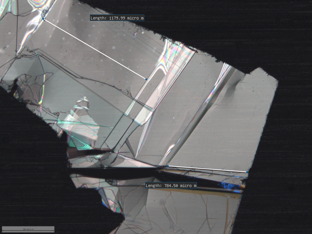
Hexagonal boron nitride (hBN) is a layered material with a crystal structure similar to graphene, composed of alternating boron and nitrogen atoms in a hexagonal lattice.
However, unlike graphene, hBN is a wide-bandgap electrical insulator (~6 eV), making it electronically inert while maintaining exceptional structural compatibility with other 2D materials.
When produced as device-grade single crystals, hBN offers several key advantages:
- Atomically flat surface
- Extremely low charge trap density
- High chemical stability
- Strong dielectric performance
- Van der Waals surface compatibility
These properties make hBN uniquely suited to support and protect sensitive 2D materials.
Providing an Atomically Perfect Substrate
One of the most important roles of hBN in 2D materials research is as a substrate.
Traditional substrates such as silicon dioxide (SiO₂) introduce surface roughness and charged impurities that disrupt electron transport in atomically thin materials.
In contrast, hBN single crystals provide:
- A smooth, lattice-regular surface
- Minimal electrostatic disorder
- Reduced phonon scattering
- Chemically inert interface conditions
This enables 2D materials placed on hBN to retain their intrinsic physical properties with minimal external interference.
Enabling Van der Waals Heterostructures
A major breakthrough in 2D materials science is the concept of van der Waals heterostructures, where different atomic layers are stacked without the need for lattice matching.
In this architecture, hBN plays a central role as a universal structural component:
- Substrate layer for device fabrication
- Encapsulation layer for environmental protection
- Dielectric spacer between active layers
- Tunnel barrier in quantum devices
Because hBN interacts with neighboring layers through weak van der Waals forces, it preserves the electronic structure of adjacent materials while providing mechanical and dielectric support.
Enhancing Electronic Transport in 2D Materials
The impact of hBN on electronic performance is particularly significant in graphene and other high-mobility systems.
When 2D materials are integrated with hBN single crystals, researchers consistently observe:
- Increased carrier mobility
- Reduced charge inhomogeneity
- Improved conductivity uniformity
- Enhanced quantum transport behavior
These improvements arise from the reduction of disorder and scattering mechanisms at the interface.
Enabling Quantum Phenomena in 2D Systems
Beyond conventional electronics, hBN plays a crucial role in enabling quantum behavior in 2D materials.
By providing an ultra-clean and stable environment, hBN allows researchers to observe and manipulate:
- Quantum Hall effects
- Moiré superlattices
- Strongly correlated electron states
- Ballistic transport regimes
- Coherent quantum interference
In many cases, these phenomena can only be reliably observed when high-quality hBN single crystals are used as supporting layers.
Optical and Photonic Advantages
In addition to electronic benefits, hBN also contributes to photonic and optoelectronic applications.
Its intrinsic properties support:
- Phonon-polariton propagation
- Nanoscale light confinement
- Deep ultraviolet band-edge emission (~215 nm)
- Stable optical environments for 2D emitters
These features make hBN an important material in nanophotonics and advanced optical engineering.
Why Device-Grade hBN Matters
The performance benefits described above depend strongly on crystal quality. Not all hBN materials are suitable for advanced 2D applications.
Device-grade hBN single crystals are characterized by:
- Large single-crystal domains
- Low defect density
- High dielectric strength
- Atomically smooth terraces
- Minimal impurity concentration
Lower-quality polycrystalline BN cannot provide the same interface performance and often limits device efficiency.
Conclusion
Hexagonal boron nitride (hBN) single crystals are a foundational material for next-generation 2D technologies. By providing an atomically smooth, electrically inert, and chemically stable environment, hBN enables 2D materials to fully realize their extraordinary physical properties.
From high-mobility graphene electronics to complex van der Waals heterostructures and emerging quantum devices, hBN is not simply a supporting material—it is a key enabler of the entire 2D materials ecosystem.
As research in atomically thin systems continues to advance, the importance of device-grade hBN single crystals will only continue to grow.