As artificial intelligence computing accelerates, data transmission speeds increase, and next-generation power electronics continue to evolve, semiconductor packaging technologies are undergoing a fundamental transformation. Conventional substrate materials are increasingly facing limitations in thermal management, electrical performance, and integration density. Against this backdrop, ceramic substrates are emerging from niche applications to become critical enabling materials for future semiconductor systems.
From AI accelerators and high-bandwidth memory (HBM) packaging to ultra-high-speed optical modules and power semiconductor devices, ceramic substrates are now recognized as one of the key foundations of advanced electronic architecture.
Why Ceramic Substrates Matter
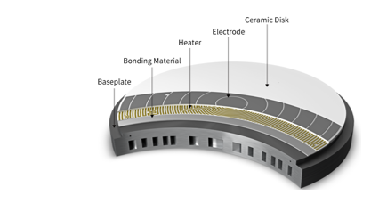
Substrates serve as the structural and electrical platform connecting chips, interconnects, and packaging systems. Historically, organic substrates and silicon-based interposers have dominated the industry. However, the rapid increase in power density and signal complexity is exposing their limitations.
Ceramic substrates offer several unique advantages:
Excellent Thermal Conductivity
Modern AI processors and high-performance computing systems generate enormous heat loads. Thermal bottlenecks can directly limit performance and reliability.
Many advanced ceramic materials—including aluminum nitride (AlN), silicon carbide (SiC), and silicon nitride (Si₃N₄)—provide significantly higher thermal conductivity than traditional organic materials. Efficient heat dissipation helps maintain device stability and supports sustained operation under high power conditions.
Low Dielectric Loss for High-Frequency Transmission
As optical communication technologies evolve toward ultra-high bandwidth and higher frequencies, signal integrity becomes increasingly critical.
Ceramic substrates possess low dielectric constants and low dielectric loss characteristics, reducing signal attenuation and improving transmission efficiency. These properties make them highly attractive for next-generation optical communication packaging and advanced AI systems.
Precise Thermal Expansion Matching
Mismatch in thermal expansion coefficients between substrate materials and semiconductor chips can create mechanical stress during repeated thermal cycling.
Ceramic materials provide thermal expansion properties that more closely align with semiconductor materials, reducing packaging stress and improving long-term reliability.
Higher Interconnect Density Potential
Advanced packaging increasingly demands finer line widths and greater integration density. Ceramic substrates can support more sophisticated interconnect architectures, enabling higher chip integration levels and smaller package footprints.
As package complexity grows, substrate technology becomes a decisive factor in overall system performance.
AI Computing Is Reshaping Packaging Requirements
The explosive growth of AI workloads has significantly increased demand for processing power and memory bandwidth.
Emerging packaging architectures require:
- Larger package sizes
- Higher input/output counts
- Improved thermal management
- Lower signal latency
- Higher integration density
Traditional packaging solutions are approaching their physical limits. Future AI systems are expected to rely increasingly on advanced substrate technologies capable of supporting large-scale heterogeneous integration.
Ceramic substrates are becoming essential because they simultaneously address electrical, thermal, and mechanical challenges.
In many next-generation AI packaging concepts, they are transitioning from optional performance enhancers to indispensable infrastructure.
Ceramic Substrates and the Evolution of Optical Modules
The rapid migration toward ultra-high-speed optical communication systems is another major driver.
Future optical modules for data centers and AI clusters require:
- Faster transmission rates
- Lower insertion loss
- Reduced power consumption
- Better thermal stability
At transmission speeds moving toward multi-terabit architectures, even minor signal degradation can affect overall system efficiency.
Ceramic substrates offer:
- superior dimensional stability
- low high-frequency loss
- improved heat dissipation capability
- long-term reliability under thermal stress
These characteristics position ceramics as strong candidates for next-generation optical packaging platforms.
Power Semiconductor Applications Continue Expanding
Power electronics are also entering a new era.
Electric vehicles, renewable energy systems, industrial automation, and high-voltage applications increasingly rely on wide-bandgap semiconductors.
These devices operate under:
- higher voltages
- higher switching frequencies
- elevated temperatures
- severe thermal cycling conditions
Ceramic substrates already play a critical role in many power modules because they combine:
- electrical insulation
- mechanical strength
- thermal conductivity
- reliability under harsh environments
As power densities continue increasing, ceramic-based substrate structures are expected to become even more important.
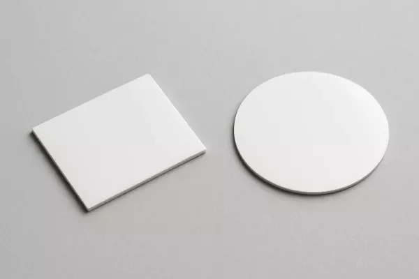
Material Platforms Driving Future Development
Several ceramic materials are attracting growing attention:
| Material | Key Characteristics | Typical Applications |
|---|---|---|
| Alumina (Al₂O₃) | Cost-effective, good insulation | General electronic packaging |
| Aluminum Nitride (AlN) | High thermal conductivity | High-power electronics |
| Silicon Nitride (Si₃N₄) | High mechanical strength | Automotive and power modules |
| Silicon Carbide (SiC) | Extreme temperature resistance | Advanced thermal management |
| Zirconia Ceramics | High toughness | Specialized structural applications |
Each material offers a different balance of thermal, electrical, and mechanical properties, allowing designers to optimize substrate selection according to application needs.
Looking Ahead: From Supporting Material to Strategic Technology
The semiconductor industry is entering a stage where material innovation increasingly determines system capability.
As AI computing expands, optical communication bandwidth rises, and power electronics continue evolving, substrate technologies are becoming strategic infrastructure rather than passive supporting components.
Ceramic substrates are uniquely positioned due to three critical strengths:
- high thermal conductivity
- low dielectric loss
- thermal expansion compatibility
These characteristics make them increasingly important for future packaging ecosystems.
Over the coming years, ceramic substrate technologies may become one of the most influential material shifts in semiconductor manufacturing, enabling the next generation of computing, communication, and power systems.