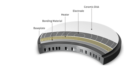
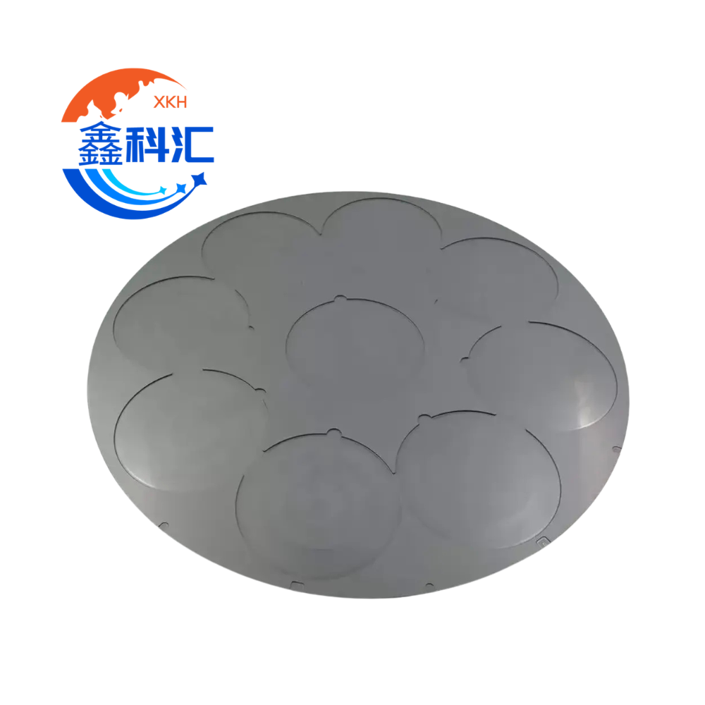
Advanced ceramics are widely used in semiconductor manufacturing equipment because of their high hardness, electrical insulation, chemical stability, wear resistance and excellent dimensional stabilit
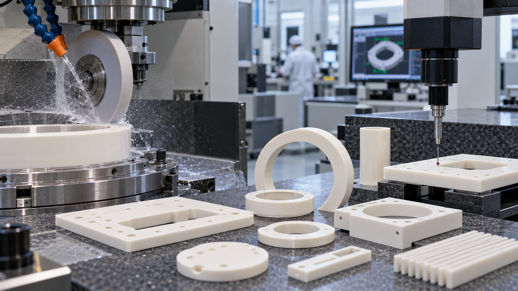
Yarı iletken ekipmanlarda kullanılan yaygın seramik malzemeler şunlardır:
- Alümina (Al₂O₃)
- Alüminyum Nitrür (AlN)
- Silisyum Karbür (SiC)
- Silisyum Nitrür (Si₃N₄)
- Zirkonya (ZrO₂)
- Yttria bazlı seramikler
- Other high-purity technical ceramics
These materials are used to manufacture components such as ceramic rings, plates, vacuum chucks, insulating parts, wafer-handling components, chamber parts, nozzles, pins and precision structural components.
However, advanced ceramics are fundamentally different from metals when it comes to machining.
They are extremely hard but also relatively brittle.
For semiconductor equipment, machining quality must therefore be evaluated not only by dimensional accuracy, but also by surface condition, edge integrity, microcracking, flatness and inspection reliability.
Four factors are especially important:
- Dimensional tolerance
- Yüzey pürüzlülüğü
- Edge chipping
- Dimensional and geometric inspection
1. Why Precision Machining Is Critical for Semiconductor Ceramic Parts
Many semiconductor ceramic components are installed close to wafers, plasma chambers, vacuum systems or high-precision motion platforms.
Small dimensional errors may affect:
- Wafer positioning
- Chamber sealing
- Plasma uniformity
- Vacuum performance
- Assembly alignment
- Thermal contact
- Elektrik yalıtımı
- Equipment repeatability
For example, a ceramic ring with an incorrect inner diameter may change the designed clearance around a wafer.
A ceramic plate with poor flatness may influence wafer support or equipment alignment.
A vacuum chuck with inconsistent surface finish may affect wafer holding and backside cleanliness.
For this reason, semiconductor ceramic machining requires a combination of material knowledge, precision grinding technology and appropriate inspection methods.
2. Why Advanced Ceramics Are Difficult to Machine
Unlike aluminum, stainless steel or other metallic materials, advanced ceramics cannot normally be machined efficiently using conventional cutting tools after full sintering.
Materials such as alumina, AlN and SiC are extremely hard.
Diamond tools are therefore commonly used for:
- Taşlama
- Drilling
- Slot machining
- Surface finishing
- Edge machining
- Lapping
- Parlatma
The main challenge is that ceramics are hard but brittle.
If machining parameters are not controlled properly, defects may include:
- Edge chipping
- Surface cracks
- Subsurface damage
- Corner breakage
- Hole breakout
- Local stress damage
These defects may not always be immediately visible but can reduce the reliability of the final component.
3. Dimensional Tolerance
Tolerance is one of the first items engineers consider when specifying a ceramic component.
However, the achievable tolerance depends on several factors.
These include:
- Ceramic material
- Component size
- Thickness
- Geometri
- Feature depth
- Hole diameter
- Wall thickness
- Machining method
- Surface-finish requirement
A simple rectangular ceramic plate may be relatively easy to control.
A thin ceramic ring with multiple holes, narrow walls and complex grooves may be considerably more difficult.
Avoid Applying the Same Tolerance Everywhere
One common design problem is assigning extremely tight tolerances to every dimension.
This can significantly increase manufacturing complexity and cost.
Instead, tolerances should be divided according to function.
Örneğin:
Kritik boyutlar
These may include:
- Wafer positioning diameter
- Mounting-hole location
- Chamber interface
- Precision alignment surface
These dimensions may require tighter control.
Non-critical dimensions
Exterior surfaces or clearance areas may allow wider tolerances.
By identifying critical dimensions clearly, engineers can improve both manufacturability and cost efficiency.
4. Flatness
Flatness is especially important for ceramic plates, vacuum chucks, heater components and wafer-handling structures.
Poor flatness may result in:
- Uneven wafer contact
- Assembly gaps
- Alignment errors
- Vacuum leakage
- Thermal-contact differences
Flatness becomes more difficult to control as component size increases and thickness decreases.
Large ceramic plates may experience deformation due to:
- Sintering stress
- Material removal
- Grinding stress
- Mounting conditions
Precision lapping and controlled grinding processes are often used when very low flatness values are required.
The required flatness should always be evaluated together with component diameter, thickness and mounting condition.
5. Parallelism
Parallelism is another critical parameter.
For components with two functional surfaces, the top and bottom faces may need to remain closely parallel.
Uygulamalar şunları içerir:
- Ceramic plates
- Spacer rings
- Yalıtım halkaları
- Vacuum chuck structures
- Wafer support platforms
Poor parallelism can create uneven assembly conditions even when each individual surface has acceptable flatness.
Therefore, flatness and parallelism should normally be specified separately.
6. Surface Roughness
Surface roughness is commonly expressed as Ra.
For semiconductor ceramic parts, surface roughness may influence:
- Parçacık üretimi
- Vacuum sealing
- Friction
- Contact stability
- Cleaning performance
- Optical appearance
- Plasma interaction
Different surfaces may require different roughness levels.
Örneğin:
A mounting surface may only require precision grinding.
A sealing surface may require finer lapping.
A wafer-contact surface may require a controlled low-roughness finish.
An optical ceramic component may require polishing.
Lower Ra Is Not Always Better
It is important to avoid specifying extremely low surface roughness without a functional reason.
Very low Ra normally requires additional processes such as fine lapping or polishing.
This increases:
- Manufacturing time
- Maliyet
- Inspection requirements
For many structural semiconductor ceramic components, a precision-ground surface may already meet functional requirements.
Surface roughness should therefore be matched to the actual application.
7. Edge Chipping
Edge chipping is one of the most common quality concerns in ceramic machining.
Ceramics are brittle materials.
When grinding or drilling reaches an edge, local stress may cause small chips to break away.
This is particularly common around:
- Outer edges
- Inner holes
- Slots
- Thin walls
- Sharp corners
The risk increases when:
- Material is very hard
- Wall thickness is small
- Hole diameter is small
- Feed rate is too aggressive
- Tool condition is poor
8. Controlling Edge Chipping
Several methods can help reduce edge damage.
Chamfers
Adding a small chamfer can significantly improve edge strength.
Instead of using a sharp 90-degree corner, the drawing may specify a controlled chamfer.
Corner Radius
A radius can also reduce stress concentration.
This is particularly useful on exposed corners.
Machining Direction
Tool path and machining direction may influence breakout around holes and slots.
Tool Selection
Diamond tool condition is extremely important.
Worn tools can increase grinding forces and edge damage.
Machining Parameters
Feed rate, spindle speed and cutting depth must be matched to the ceramic material.
9. Hole Machining
Precision holes are common in semiconductor ceramic parts.
They may be used for:
- Fasteners
- Vacuum passages
- Gas distribution
- Alignment pins
- Electrical connections
Important hole specifications include:
- Diameter
- Position tolerance
- Roundness
- Concentricity
- Hole-to-edge distance
- Surface condition
Very small holes or holes close to component edges require particular attention.
Insufficient edge distance may significantly increase the risk of cracking or chipping.
Designers should therefore confirm machining feasibility before finalizing thin-wall or closely spaced hole structures.
10. Thin Walls and Narrow Features
Thin ceramic sections can be especially difficult to machine.
Narrow walls may be damaged during:
- Taşlama
- Drilling
- Temizlik
- Transportation
- Installation
Where possible, designs should avoid unnecessarily thin unsupported sections.
If thin-wall geometry is unavoidable, machining sequence and fixturing must be carefully planned.
This is especially relevant for:
- Ceramic rings
- Multi-hole components
- Slotted parts
- Thin spacers
11. Concentricity and Roundness
Ceramic rings and cylindrical parts often require control of concentricity and roundness.
These parameters are important for:
- Wafer-centered structures
- Odak halkaları
- Chamber rings
- Rotating assemblies
- Cylindrical insulating components
A ring may have correct inner and outer diameters but still fail if these diameters are not concentric.
Therefore, diameter tolerance alone is not always sufficient.
Geometric tolerances should be defined according to functional requirements.
12. Dimensional Inspection
Inspection is a critical part of semiconductor ceramic manufacturing.
Depending on the component and tolerance, measurement equipment may include:
- Digital calipers
- Micrometers
- Height gauges
- Optical comparators
- Coordinate Measuring Machines
- Surface profilometers
- Flatness measurement systems
- Optical inspection equipment
For high-precision components, CMM inspection is often used to verify complex geometry and positional tolerances.
13. Surface Roughness Inspection
Surface roughness should be verified using appropriate measuring equipment.
The measurement direction and location are important.
Different areas of the same component may produce different Ra values.
For this reason, drawings should ideally identify which surfaces require roughness control.
Typical drawing notation may include:
Ra ≤ X μm
or
Ra ≤ X nm
depending on application.
Extremely low nanometer-level roughness normally requires polishing rather than conventional grinding.
14. Flatness Inspection
Flatness may be measured using several methods depending on component size and tolerance.
These may include:
- Dial indicator scanning
- Precision granite reference surfaces
- CMM measurement
- Optical flat measurement
- Interferometric measurement
The correct inspection method should match the required tolerance.
For extremely tight flatness requirements, measurement environment and temperature can also become important.
15. Visual Inspection and Edge Quality
Not all defects are dimensional.
Visual inspection may be used to identify:
- Edge chips
- Cracks
- Surface scratches
- Grinding marks
- Discoloration
- Contamination
For semiconductor equipment parts, acceptable chip size and cosmetic standards should ideally be defined.
A simple requirement such as “no chipping” may be difficult to interpret consistently.
Instead, the specification may define:
- Maximum chip width
- Maximum chip depth
- Prohibited locations
- Crack acceptance criteria
Clear acceptance standards help reduce disagreements during quality inspection.
16. Sintered Size vs. Finished Size
Ceramic parts usually shrink during sintering.
Therefore, components are often manufactured in two stages.
Near-Net-Shape Manufacturing
The ceramic body is formed and sintered close to the required geometry.
Final Precision Machining
Critical dimensions are then finished using diamond grinding, lapping or polishing.
For semiconductor equipment, final machining is particularly important because sintering alone normally cannot provide the required precision for all critical features.
Design engineers should therefore understand that the final geometry depends on machining allowance and finishing strategy.
17. Material Differences in Machining
Different ceramics behave differently during machining.
Alümina
Alumina is widely used and has mature machining technology.
It offers good dimensional stability and wear resistance but still requires careful diamond grinding.
Alüminyum Nitrür
AlN combines electrical insulation with high thermal conductivity.
Its machining requires careful control to avoid surface damage and contamination.
Silisyum Karbür
SiC is extremely hard.
It provides excellent stiffness and dimensional stability but is more challenging to machine.
Tool wear and machining cost may therefore be higher compared with alumina.
Silisyum Nitrür
Silicon nitride offers excellent mechanical strength and fracture toughness compared with many other ceramics.
However, its high hardness still requires specialized grinding methods.
18. Designing for Ceramic Machinability
Good ceramic component design should consider manufacturing feasibility from the beginning.
Recommended design practices include:
- Avoid unnecessary sharp corners
- Add chamfers where possible
- Maintain sufficient hole-to-edge distance
- Avoid extremely thin unsupported walls
- Identify critical dimensions
- Apply tight tolerances only where necessary
- Specify functional surface roughness
- Clearly define inspection datums
Design optimization can significantly improve yield and reduce machining cost.
19. Information Required for a Custom Ceramic Machining RFQ
For custom semiconductor ceramic parts, customers should ideally provide:
- 2D drawing
- 3D CAD file
- Malzeme
- Material purity
- Overall dimensions
- Critical tolerances
- Flatness
- Parallelism
- Concentricity
- Position tolerance
- Yüzey pürüzlülüğü
- Chamfer requirements
- Edge-chipping criteria
- Hole dimensions
- Çalışma sıcaklığı
- Vacuum or plasma environment
- Miktar
The intended application should also be explained.
Örneğin:
Alumina insulating ring for plasma equipment
is more informative than simply requesting an alumina ring.
20. Precision Ceramic Machining for Semiconductor Equipment
Machining advanced ceramics for semiconductor equipment requires more than achieving nominal dimensions.
A high-quality ceramic component must also control:
- Yüzey pürüzlülüğü
- Flatness
- Parallelism
- Edge integrity
- Hole quality
- Concentricity
- Dimensional repeatability
These factors directly influence equipment assembly, wafer handling, vacuum performance and long-term reliability.
XKH Ceramics provides precision-machined ceramic components based on customer drawings and application requirements.
Available materials include:
- Alümina
- Alüminyum Nitrür
- Silisyum Karbür
- Silisyum Nitrür
- Other advanced ceramic materials
Custom processing can include:
- Hassas taşlama
- Hole machining
- Slot machining
- Lapping
- Parlatma
- Edge finishing
- Boyutsal denetim
For new semiconductor ceramic projects, providing the drawing, ceramic material, critical tolerances, surface roughness and application information allows manufacturing feasibility to be evaluated more accurately.