Advanced ceramics have become indispensable materials in modern semiconductor equipment. Components used in plasma etching, chemical vapor deposition (CVD), physical vapor deposition (PVD), ion implantation, and wafer handling systems must operate reliably under extreme conditions, including high-energy plasma exposure, corrosive process gases, elevated temperatures, thermal cycling, and high-voltage electrical fields.
Materials such as alumina (Al₂O₃), aluminum nitride (AlN), silicon carbide (SiC), and silicon nitride (Si₃N₄) offer exceptional hardness, electrical insulation, thermal stability, and plasma resistance. However, these same properties also make them among the most difficult engineering materials to manufacture.
As semiconductor devices continue to evolve toward higher integration and smaller process nodes, ceramic components are becoming increasingly complex. Traditional simple shapes are being replaced by thin-wall structures, multi-channel designs, micro-hole arrays, and intricate three-dimensional geometries.
This article explores the key manufacturing challenges of complex semiconductor ceramic components and the advanced technologies used to overcome them.
Typical Complex Ceramic Components in Semiconductor Equipment
Modern semiconductor tools require ceramic parts with highly demanding geometries, including:
Elektrostatik Aynalar (ESC)
Electrostatic chucks often incorporate:
- Yüksek yoğunluklu mikro delik dizileri
- Complex backside gas channels
- Precision support mesas
- Embedded heating structures
These features are essential for achieving uniform wafer clamping and temperature control.
Aşındırma Odası Bileşenleri
Plasma etching systems utilize ceramic parts such as:
- Showerheads
- Odak halkaları
- Yalıtım halkaları
- Gaz dağıtım plakaları
These components commonly feature curved surfaces, varying wall thicknesses, flange structures, and thousands of precision holes.
Sensor Housings and Precision Ceramic Assemblies
Advanced sensors used in semiconductor equipment may require:
- Thin-wall ceramic housings
- Internal cavities
- Threaded interfaces
- Micro-feedthrough openings
Manufacturing these structures without introducing defects presents significant technical challenges.
Challenge 1: Forming Complex Ceramic Green Bodies
The forming stage determines the initial geometry and density distribution of the ceramic component. Any density variation introduced during forming may result in distortion, cracking, or dimensional deviation after sintering.
Traditional dry pressing and slip casting often struggle to meet the requirements of highly customized semiconductor ceramic parts.
Several advanced forming technologies are commonly used.
Gel Casting
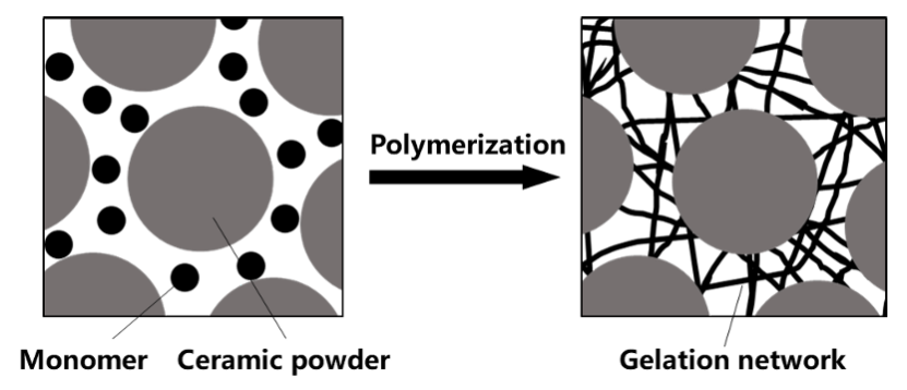
Gel casting combines low-viscosity ceramic slurries with in-situ polymerization.
Avantajları şunlardır:
- Near-net-shape manufacturing
- Excellent density uniformity
- Minimal drying distortion
- Reduced machining requirements
Because ceramic particles are immobilized within a three-dimensional polymer network, sedimentation and density gradients are significantly reduced. This makes gel casting especially suitable for large and thin-wall semiconductor ceramic components.
Ceramic Injection Molding (CIM)
Ceramic Injection Molding mixes ceramic powder with binders and plasticizers to create feedstock that can be injected into precision molds.
Key benefits include:
- Yüksek boyut hassasiyeti
- Excellent repeatability
- Uniform green density
- Uygun maliyetli seri üretim
CIM is widely used for manufacturing small and intricate components such as sensor housings, ceramic insulators, and miniature rings.
Cold Isostatic Pressing (CIP)
For axisymmetric components such as focus rings, cold isostatic pressing provides highly uniform compaction pressure in all directions.
Avantajlar şunları içerir:
- Improved density uniformity
- Reduced internal stress
- Daha iyi boyutsal tutarlılık
This method helps minimize defects caused by pressure gradients that often occur in conventional pressing processes.
Ceramic 3D Printing
Advanced additive manufacturing technologies such as:
- Digital Light Processing (DLP)
- Direct Ink Writing (DIW)
allow fabrication of internal channels and geometries that are impossible to achieve using traditional tooling.
Ceramic 3D printing is particularly attractive for prototype electrostatic chucks with integrated cooling channels and highly customized semiconductor ceramic designs.
Challenge 2: Controlling Distortion During Sintering
Sintering transforms porous green bodies into dense ceramic components. During this process, ceramics typically undergo 15%–25% linear shrinkage.
For complex geometries, non-uniform shrinkage can lead to:
- Warpage
- Cracking
- Collapse of thin-wall structures
- Dimensional inaccuracies
Therefore, advanced sintering technologies are critical.
Hot Press Sintering
Hot pressing applies external pressure during densification.
Avantajları şunlardır:
- Lower sintering temperatures
- Reduced grain growth
- Higher density
- Better shape retention
This method is commonly used for high-performance electrostatic chucks and plasma-resistant ceramic components.
Gas Pressure Sintering
Gas pressure sintering utilizes high-pressure inert gases to suppress material decomposition and eliminate residual porosity.
Avantajlar şunları içerir:
- Improved densification
- Reduced closed pores
- Enhanced mechanical properties
- Daha iyi boyutsal kararlılık
Spark Plasma Sintering (SPS)
SPS employs pulsed direct current to generate rapid internal heating.
Temel avantajlar şunlardır:
- Extremely fast densification
- Uniform temperature distribution
- Reduced grain growth
- Lower distortion
SPS is particularly suitable for small, high-precision semiconductor ceramic components.
Microwave Sintering
Unlike conventional furnace heating, microwave sintering generates volumetric heating throughout the material.
Avantajlar şunları içerir:
- Faster heating rates
- Azaltılmış termal gradyanlar
- Daha düşük enerji tüketimi
- Minimized warpage and cracking
Challenge 3: Precision Machining of Hard and Brittle Ceramics
Even after sintering, semiconductor ceramic components often require ultra-precision finishing to achieve:
- Sub-micron dimensional tolerances
- Nanometer-level surface roughness
- High edge quality
- Defect-free microstructures
However, the extreme hardness and brittleness of ceramics make conventional machining extremely challenging.
Common issues include:
- Tool wear
- Edge chipping
- Surface microcracks
- Subsurface damage
To overcome these limitations, several advanced finishing technologies have emerged.
Abrasive Flow Machining (AFM)
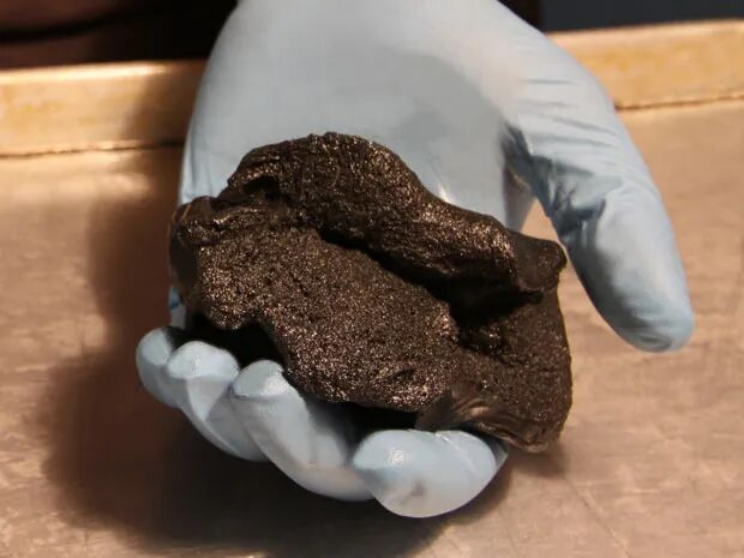
AFM utilizes a semi-solid abrasive media forced through internal channels and micro-holes.
This process is particularly effective for:
- Showerhead hole finishing
- Gas distribution channels
- ESC backside gas paths
AFM removes burrs while creating smooth and uniform internal surfaces.
Laser Drilling and Laser Polishing
Femtosecond and picosecond laser systems enable:
- Precision micro-hole correction
- Crack-free machining
- Minimal heat-affected zones
Laser polishing can also improve surface finish on complex three-dimensional structures and enclosed cavities inaccessible to conventional tools.
Magnetorheological Finishing (MRF)
MRF employs a magnetic field to control a polishing fluid containing abrasive particles.
Avantajları şunlardır:
- High surface accuracy
- Excellent process control
- Low subsurface damage
- Suitability for complex surfaces
The technology is widely used for precision ceramic components requiring exceptional surface integrity.
Plasma Assisted Polishing (PAP)
PAP combines plasma surface modification with gentle mechanical polishing.
Avantajlar şunları içerir:
- Atomic-level surface finishing
- High material removal efficiency
- Minimal subsurface damage
- Uniform treatment of microstructures and internal features
This emerging technology is attracting growing interest in semiconductor ceramic manufacturing.
Future Outlook for Semiconductor Ceramic Manufacturing
As semiconductor equipment becomes more sophisticated, demand for advanced ceramic components with complex geometries will continue to increase.
Successfully manufacturing these components requires seamless integration of:
- Advanced forming technologies
- Precision-controlled sintering processes
- Ultra-precision finishing methods
By overcoming the inherent challenges associated with hard and brittle ceramic materials, manufacturers can unlock the full potential of alumina, aluminum nitride, silicon carbide, and silicon nitride ceramics for next-generation semiconductor equipment.
At Xinkehui, we specialize in the custom manufacturing of precision semiconductor ceramic components, including electrostatic chucks, focus rings, showerheads, insulating components, and plasma-resistant ceramic parts. Through advanced forming, sintering, and precision machining technologies, we deliver high-performance ceramic solutions tailored to demanding semiconductor applications.