
Vacuum chucks are essential components in modern semiconductor manufacturing. They securely hold silicon, silicon carbide (SiC), sapphire, glass, and compound semiconductor wafers during lithography, inspection, grinding, polishing, laser processing, metrology, and wafer bonding.
Among various chuck technologies, porous ceramic vacuum chuck have become the preferred solution because they provide uniform vacuum distribution, excellent dimensional stability, high cleanliness, and outstanding wear resistance.
However, not all ceramic vacuum chucks deliver the same performance. Their ability to securely hold ultra-flat wafers depends on several engineering parameters, including porosity, flatness, material selection, vacuum distribution, and machining accuracy.
This article explains how these design factors influence wafer holding performance and what engineers should consider when selecting a ceramic vacuum chuck.
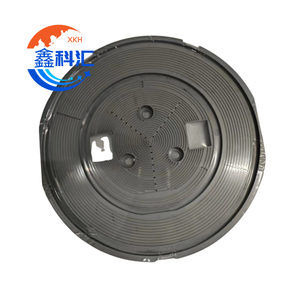
What Is a Ceramic Vacuum Chuck?
A ceramic vacuum chuck is a precision fixture that uses negative pressure to hold a wafer against a highly flat ceramic surface.
Instead of relying on mechanical clamps, vacuum is distributed through internal channels or microscopic pores, creating a uniform holding force across the wafer.
Ceramic vacuum chucks are widely used for:
- Semiconductor lithography
- Wafer grinding
- CMP
- Kontrola wafli
- Wafer bonding
- Laser processing
- Thin wafer handling
- MEMS manufacturing
- Advanced packaging
Depending on the application, the chuck may be manufactured from:
- High-purity alumina (Al₂O₃)
- Azotek glinu (AlN)
- Silicon carbide ceramic
- Porous alumina
- Porous silicon carbide
Why Porosity Matters
One of the most important characteristics of a ceramic vacuum chuck is its porosity.
Unlike conventional vacuum chucks that rely on machined vacuum grooves, porous ceramic chucks distribute vacuum through millions of microscopic interconnected pores.
This provides several advantages.
Uniform Vacuum Distribution
The vacuum force is evenly distributed over the entire wafer instead of being concentrated along grooves.
Korzyści obejmują:
- Better wafer flatness
- Reduced local stress
- Less deformation
- More consistent positioning
This is especially important for:
- 300 mm wafers
- Thin wafers
- Wafle szafirowe
- Glass wafers
- Wafle SiC
Zmniejszone generowanie cząstek
Mechanical groove edges may trap contaminants or generate particles during repeated loading.
Porous ceramic surfaces minimize these issues because the vacuum is distributed internally.
Lower particle generation improves process yield, especially in cleanroom environments.
Improved Wafer Stability
Uniform suction reduces wafer movement during:
- High-speed polishing
- Laser machining
- Kontrola wafli
- High-speed spindle rotation
Even slight wafer movement can significantly affect dimensional accuracy.
Selecting the Right Porosity
Higher porosity is not always better.
If porosity is too high:
- Vacuum leakage increases.
- Holding force decreases.
- Mechanical strength is reduced.
If porosity is too low:
- Airflow becomes insufficient.
- Vacuum builds slowly.
- Wafer loading efficiency decreases.
Manufacturers typically optimize pore size and porosity according to:
- Wafer diameter
- Wafer thickness
- Materiał
- Vacuum pressure
- Wymagania dotyczące wykończenia powierzchni
Why Flatness Is Critical
The chuck surface acts as the reference plane for nearly every precision wafer process.
If the chuck surface is not sufficiently flat, the wafer will deform during vacuum loading.
Common consequences include:
- Lithography overlay errors
- Grinding thickness variation
- CMP non-uniformity
- Bonding voids
- Metrology inaccuracies
For semiconductor applications, chuck flatness is often controlled within only a few micrometers over the entire working area.
Ultra-precision applications may require sub-micrometer flatness.
Surface Finish and Wafer Contact
Surface roughness affects both vacuum sealing and particle generation.
An excessively rough surface creates air leakage paths.
An excessively smooth surface may increase wafer sticking during unloading.
Manufacturers therefore optimize surface roughness to balance:
- Vacuum sealing
- Wafer release
- Particle control
- Odporność na zużycie
Diamond grinding and precision lapping are commonly used to achieve consistent surface quality.
Wybór materiału
Ceramika z tlenku glinu
Zalety:
- Excellent rigidity
- High wear resistance
- Cost-effective
- Good electrical insulation
Typical applications:
- Sprzęt inspekcyjny
- Szlifowanie
- CMP
Azotek glinu
Zalety:
- Wysoka przewodność cieplna
- Low thermal expansion mismatch
- Doskonała odporność na działanie plazmy
Typical applications:
- Wafer bonding
- Przetwarzanie termiczne
- High-power semiconductor manufacturing
Ceramika z węglika krzemu
Zalety:
- Extremely high stiffness
- Wyjątkowa stabilność termiczna
- Doskonała odporność chemiczna
- Low thermal deformation
Typical applications:
- High-temperature processing
- Precision inspection
- Advanced packaging
Vacuum Groove Design vs Porous Design
Traditional groove-type chucks remain suitable for many applications.
However, porous ceramic designs provide several performance advantages.
| Cecha | Groove Chuck | Porous Ceramic Chuck |
|---|---|---|
| Vacuum distribution | Localized | Uniform |
| Generowanie cząstek | Wyższy | Niższy |
| Thin wafer support | Umiarkowany | Doskonały |
| Flatness consistency | Dobry | Doskonały |
| Air leakage | Umiarkowany | Niski |
| Wafer deformation | Wyższy | Niższy |
For ultra-thin wafers and fragile compound semiconductor substrates, porous ceramic chucks generally provide better holding stability.
Challenges in Thin Wafer Processing
As semiconductor devices continue to shrink, wafer thickness continues to decrease.
Modern wafers may be:
- 300 μm
- 200 μm
- 150 μm
- 100 μm
- Below 50 μm
These wafers are extremely susceptible to:
- Warpage
- Bow
- Cracking
- Chipping
- Local deformation
A properly designed ceramic vacuum chuck minimizes these risks by providing evenly distributed support.
Design Considerations
When designing a ceramic vacuum chuck, engineers should evaluate:
Wafer diameter
Different chuck layouts are required for:
- 4 inch
- 6 inch
- 8 inch
- 12 inch wafers
Vacuum channel layout
Proper channel design ensures:
- Uniform pressure
- Fast vacuum response
- Stable holding
Pore size
Pore diameter influences:
- Airflow
- Leakage
- Vacuum stability
- Surface strength
Rozszerzalność cieplna
For high-temperature applications, the thermal expansion coefficient should closely match the wafer material whenever possible.
Mechanical rigidity
The chuck must resist bending under:
- Vacuum loading
- Machine vibration
- Rotational forces
Surface coating
Some applications use specialized coatings to improve:
- Odporność chemiczna
- Odporność na zużycie
- Plasma durability
Typowe zastosowania
Ceramic vacuum chucks are widely used in:
- Wafer grinding systems
- CMP equipment
- Lithography tools
- Wafer inspection systems
- Laser dicing
- Wafer bonding
- Metrology equipment
- Optical inspection
- Semiconductor packaging
- MEMS manufacturing
What Buyers Should Ask Suppliers
Before purchasing a ceramic vacuum chuck, engineers should confirm:
- Ceramic material
- Czystość
- Porosity
- Pore size
- Flatness specification
- Surface roughness (Ra)
- Parallelism
- Vacuum leakage rate
- Working temperature
- Maximum wafer size
- Vacuum hole layout
- Cleaning compatibility
- Odporność na plazmę
- Custom machining capability
Wnioski
The performance of a ceramic vacuum chuck depends on much more than its external dimensions. Porosity, flatness, surface finish, material properties, and vacuum distribution all influence wafer holding stability and process accuracy.
As semiconductor wafers become thinner, larger, and more delicate, porous ceramic vacuum chucks provide significant advantages in reducing deformation, minimizing particle contamination, and improving process consistency. Selecting the right chuck design for the specific wafer material and manufacturing process is essential for achieving high yield and long-term equipment reliability.
FAQ
What is the advantage of a porous ceramic vacuum chuck?
A porous ceramic vacuum chuck distributes vacuum evenly through microscopic pores, providing uniform wafer support, lower particle generation, and reduced deformation compared with traditional grooved vacuum chucks.
Which ceramic material is best for semiconductor vacuum chucks?
The optimal material depends on the application. Alumina offers excellent rigidity and cost-effectiveness, aluminum nitride provides superior thermal conductivity, and silicon carbide ceramic delivers exceptional stiffness, thermal stability, and chemical resistance.
Why is flatness important for a vacuum chuck?
The chuck surface serves as the reference plane for wafer processing. Poor flatness can introduce wafer deformation, resulting in lithography overlay errors, non-uniform grinding, bonding defects, and reduced process accuracy.
Can ceramic vacuum chucks be customized?
Yes. Manufacturers commonly offer custom designs based on wafer diameter, vacuum hole pattern, porosity, material selection, flatness requirements, and equipment interface dimensions.

