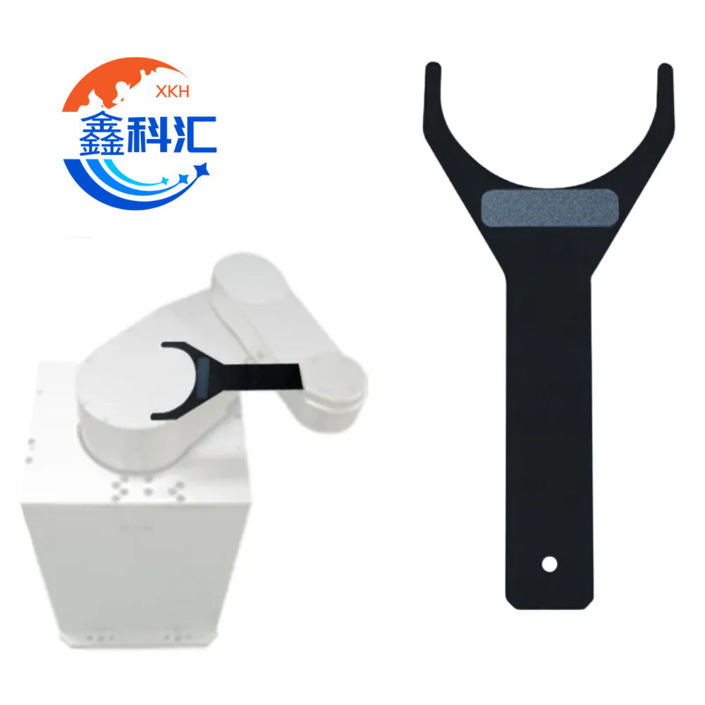
Hoe geavanceerde keramiek de prestaties van halfgeleiderapparatuur verbetert
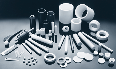
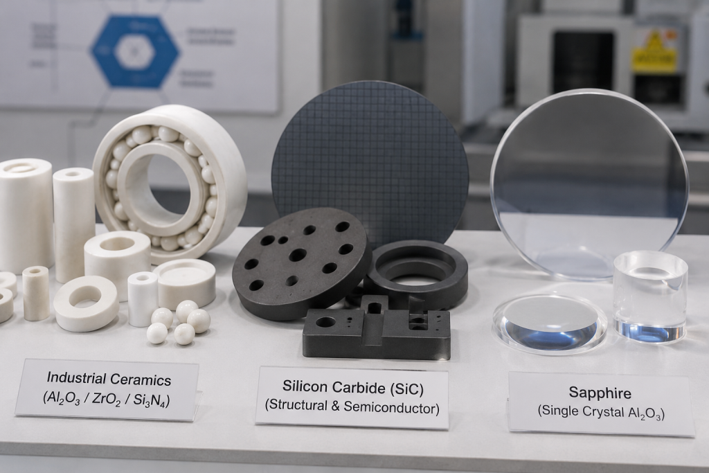
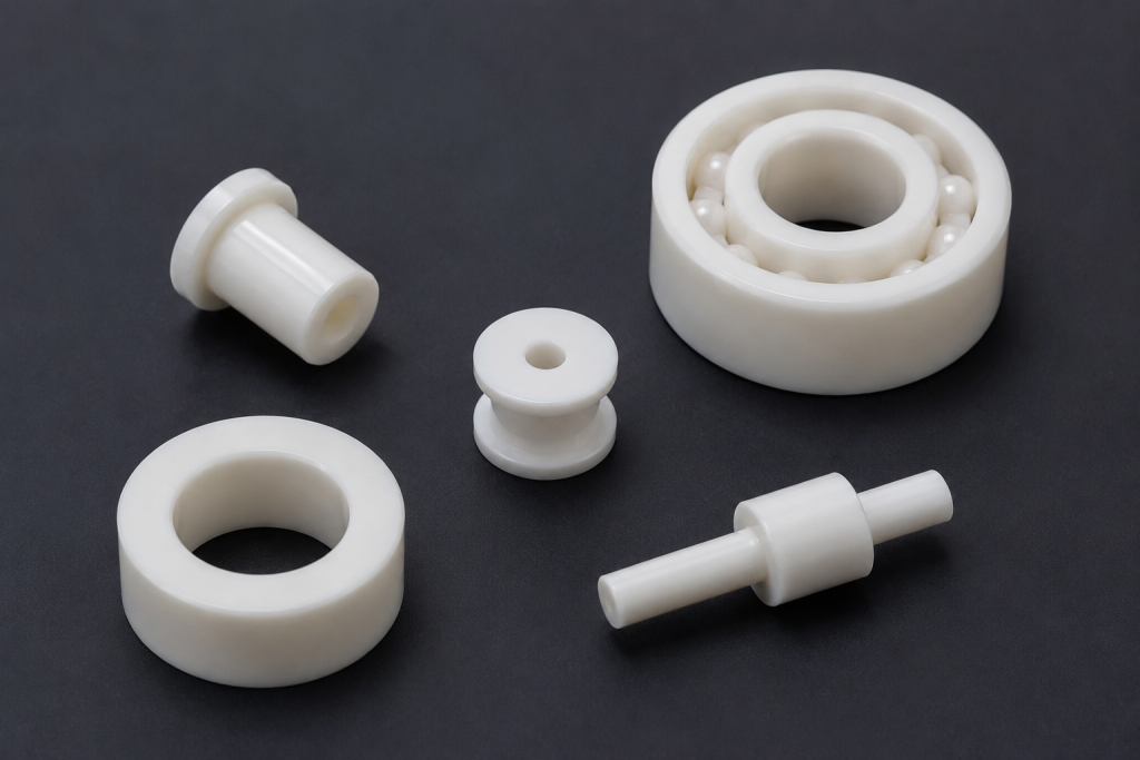
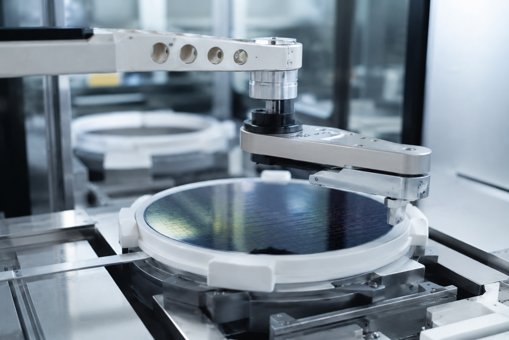
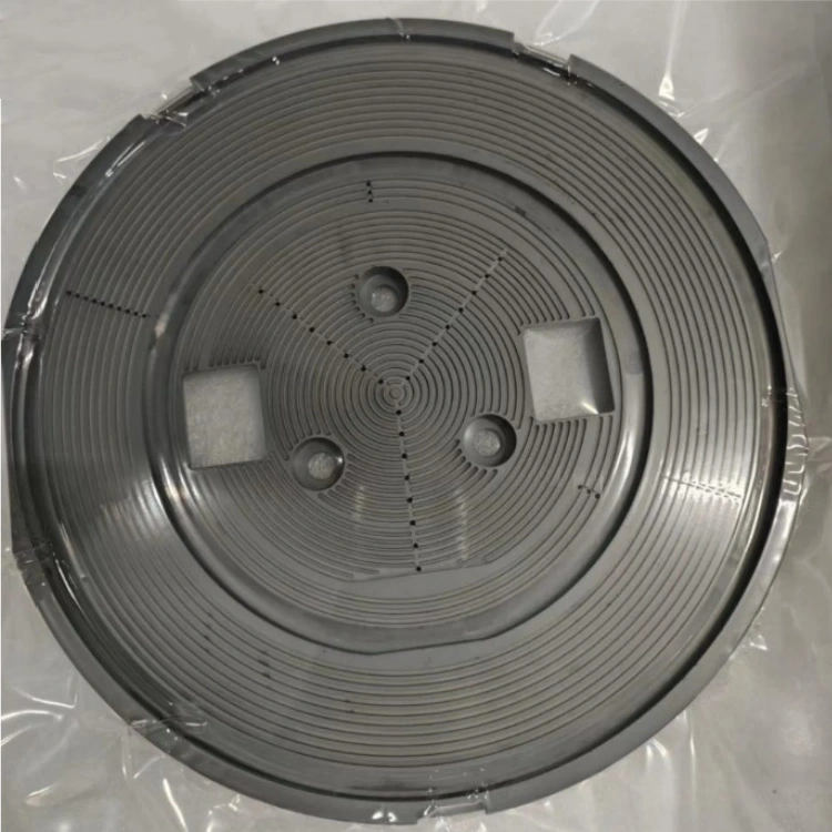
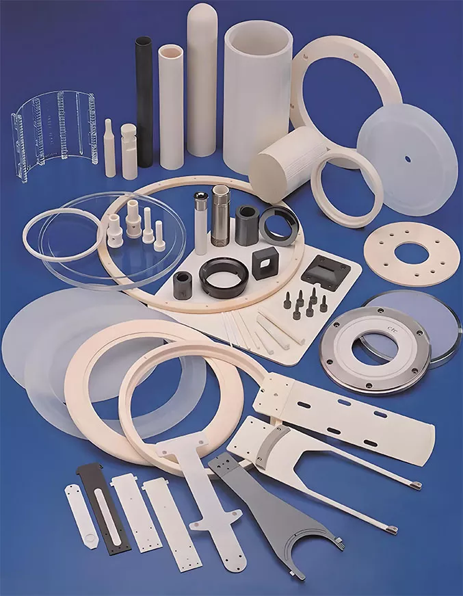
The semiconductor industry operates at the limits of precision engineering. Modern fabrication processes require extreme temperatures, highly reactive chemicals, plasma exposure, vacuum environments, and contamination control at microscopic scales. As integrated circuits continue advancing toward smaller process nodes and larger wafer sizes, equipment performance requirements become increasingly demanding. Under these conditions, material selection becomes a […]
Hoe geavanceerde keramiek de prestaties van halfgeleiderapparatuur verbetert Meer lezen »