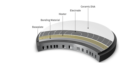
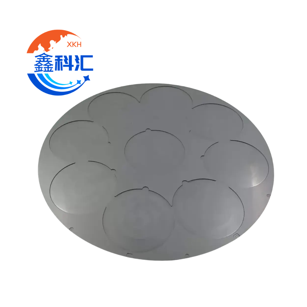
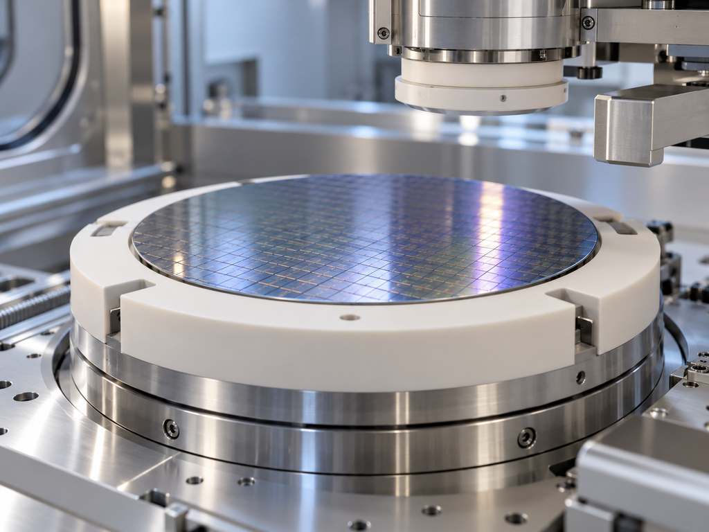
Precision ceramic wafer chucks and wafer clamps are widely used in semiconductor equipment to support, position and hold wafers during processing, inspection and handling.
As wafer sizes increase and semiconductor manufacturing tolerances become tighter, the dimensional stability and surface quality of these components become increasingly important.
Advanced ceramics are particularly suitable for wafer handling applications because they combine high stiffness, thermal stability, wear resistance and chemical resistance.
Why Ceramics Are Used for Wafer Handling
Metal components can be suitable for many mechanical applications, but semiconductor equipment often operates under conditions involving vacuum, elevated temperatures, plasma and corrosive gases.
Advanced ceramics provide several advantages:
- 높은 치수 안정성
- 전기 절연
- 뛰어난 내마모성
- High-temperature performance
- Low thermal expansion options
- Resistance to chemical attack
- Good surface finish capability
These properties make ceramic components suitable for precision wafer support and positioning.
일반적인 세라믹 재료
Three common materials for semiconductor wafer chucks and clamps are alumina, aluminum nitride and silicon carbide.
알루미나
Alumina ceramic is widely used because of its electrical insulation, mechanical strength and mature manufacturing process.
It is often selected for wafer holders, support plates, insulating components and precision ceramic structures.
질화 알루미늄
Aluminum nitride is preferred when thermal conductivity is important.
It provides both electrical insulation and efficient heat transfer, making it suitable for wafer platforms and components used near temperature-controlled processing areas.
실리콘 카바이드
Silicon carbide offers excellent stiffness, wear resistance and high-temperature stability.
It can be used in demanding wafer handling or processing environments where mechanical stability is critical.
Wafer Chuck and Clamp Design
A ceramic wafer chuck or clamp may appear simple, but many designs include complex functional features.
Typical structures can include:
- Vacuum holes
- Vacuum grooves
- Gas channels
- Wafer locating features
- Edge support structures
- Mounting holes
- Precision pockets
- Lift pin holes
These features must often be machined with tight positional and dimensional tolerances.
The surface condition is also important. Excessive roughness or poor edge finishing can increase the risk of particles or wafer damage.
Flatness and Precision
Flatness is one of the most important specifications for wafer support components.
If the supporting surface is uneven, the wafer may experience local stress or poor positioning.
For inspection, lithography or other precision applications, even small deviations can affect measurement or process accuracy.
Manufacturers therefore need to carefully control:
- 평탄도
- 병렬 처리
- 두께
- Hole position
- 표면 거칠기
- Edge geometry
- Chamfers
- Concentricity
Precision grinding, lapping and polishing may be used depending on the application.
맞춤형 세라믹 부품
Semiconductor equipment manufacturers frequently require custom rather than standard ceramic parts.
Design requirements may vary according to wafer size, equipment architecture, process temperature and vacuum environment.
Typical wafer sizes include 100mm, 150mm, 200mm and 300mm, while customized systems may use other dimensions.
A qualified ceramic supplier should be able to work from drawings, STEP files or application requirements and provide recommendations on material selection and machining feasibility.
As semiconductor equipment continues to move toward higher precision and greater automation, advanced ceramic wafer chucks, clamps and handling components will play an increasingly important role in maintaining process stability and wafer protection.