As semiconductor devices continue evolving toward smaller nodes, higher integration density, and greater processing precision, the demand for ultra-clean, heat-resistant, and plasma-stable materials inside semiconductor equipment has increased significantly. Among advanced engineering ceramics, high-purity alumina ceramic (Al₂O₃) remains one of the most widely used materials across semiconductor manufacturing systems.
From plasma etching chambers to wafer handling systems and thermal processing equipment, alumina ceramic components provide excellent electrical insulation, mechanical stability, wear resistance, and corrosion protection under harsh operating conditions.
Today, high-purity alumina ceramics are extensively used in semiconductor fabrication equipment including etching systems, deposition tools, CMP platforms, ion implantation systems, diffusion furnaces, and wafer transfer modules.
Why Alumina Ceramics Are Important in Semiconductor Manufacturing
Semiconductor fabrication involves multiple highly controlled processes such as:
- Plasma etching
- Thin film deposition
- Photolithography
- Chemical mechanical polishing (CMP)
- Ion implantation
- Thermal annealing
- Oxidation and diffusion
These processes expose internal equipment components to:
- High-energy plasma
- Vacuum environments
- Corrosive gases and chemicals
- High temperatures
- Mechanical wear and vibration
Traditional metal materials often struggle in such environments due to contamination risks, thermal expansion, or chemical instability. High-purity alumina ceramics solve many of these challenges through their unique combination of properties.
Key Properties of High-Purity Alumina Ceramics
High-purity alumina used in semiconductor equipment generally exceeds 99.5% purity and offers:
Excellent Electrical Insulation
Alumina maintains high electrical resistivity even at elevated temperatures, making it ideal for plasma chambers and electrostatic systems.
Outstanding Plasma Resistance
The material demonstrates strong resistance to plasma erosion and chemical attack in fluorine- and chlorine-based environments.
High Mechanical Strength
Alumina ceramics provide excellent rigidity, hardness, and structural stability under demanding operating conditions.
Superior Wear Resistance
Low wear characteristics make alumina suitable for moving mechanical assemblies and wafer contact components.
High Temperature Stability
Alumina performs reliably in vacuum and high-temperature processing environments commonly found in semiconductor equipment.
Main Applications of Alumina Ceramics in Semiconductor Processes
1. Plasma Etching Systems
In plasma etching equipment, alumina ceramics are commonly used for:
- Chamber liners
- Plasma shields
- Focus rings
- Edge protection components
These parts help reduce contamination and protect chamber structures from plasma erosion.
2. Thin Film Deposition Equipment
In CVD, PECVD, and PVD systems, alumina ceramics are widely used in:
- Electrostatic chucks (ESC)
- Ceramic heaters
- Chamber insulation structures
- Gas distribution assemblies
Their thermal stability and insulation performance help maintain uniform deposition conditions.
3. Chemical Mechanical Polishing (CMP)
CMP processes require components with:
- Low wear rates
- Chemical resistance
- Dimensional stability
Alumina ceramic components used in CMP equipment include:
- Polishing plates
- Vacuum chucks
- Transfer arms
- Guide structures
4. Ion Implantation & Thermal Processing
In ion implantation, annealing, oxidation, and diffusion systems, alumina ceramics are used because of their:
- Thermal resistance
- Electrical insulation
- Structural reliability
These properties support stable wafer processing under high-temperature conditions.
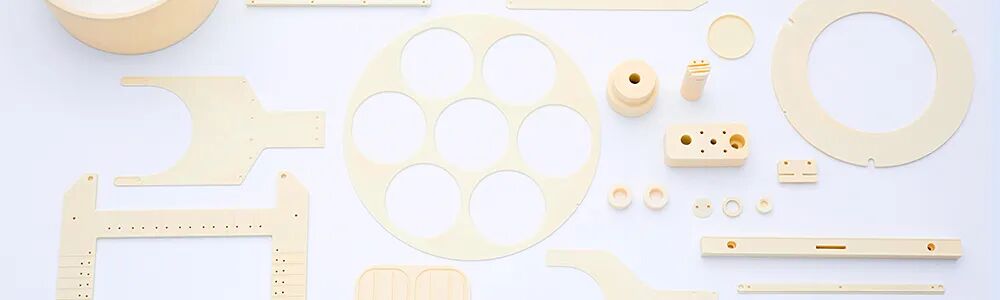
Common Alumina Ceramic Components in Semiconductor Equipment
Ring & Cylindrical Components
This category includes:
- Focus rings
- Edge rings
- Protection rings
- Chamber liners
- Insulation cylinders
- Thermal protection tubes
These components are mainly used to:
- Control plasma distribution
- Protect chamber structures
- Improve process stability
Gas Flow Management Components
Ceramic Nozzles
Used for process gas delivery and directional gas control in deposition and etching chambers.
Gas Distribution Plates
Help maintain uniform gas flow and stable plasma density across the wafer surface.
Nozzle Covers
Support gas injection assemblies while also reducing residue accumulation inside the chamber.
Structural & Support Components
Wafer Support Platforms
Used as carrier structures for wafers during processing.
Lift Pins
Enable wafer loading and unloading inside semiconductor chambers.
Ceramic Guide Rails & Bearings
Support precise mechanical movement while maintaining wear resistance and insulation.
Ceramic Fasteners
Ceramic screws and fastening parts replace metals in high-temperature or electrically isolated areas.
Wafer Handling & Insulation Components
Wafer Handling Arms
High-strength ceramic robotic arms are used for wafer transfer inside vacuum environments.
Ceramic Insulation Plates
Prevent unwanted electrical conduction between chamber structures.
Ceramic Heat Dissipation Parts
Assist with thermal management and localized cooling.
Advanced Alumina Ceramic Modules
Vacuum Chucks
Vacuum chucks hold wafers flat through vacuum suction during:
- Etching
- CMP
- Inspection processes
Integrated cooling channels help improve thermal control and process consistency.
Electrostatic Chucks (ESC)
Electrostatic chucks use electrostatic force to hold wafers during plasma processing.
Alumina ceramics are widely used because they provide:
- Electrical insulation
- Plasma resistance
- Thermal stability
ESC systems are essential in advanced etching and deposition equipment.
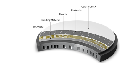
Ceramic Heaters
Ceramic heaters provide stable and uniform wafer heating in:
- Deposition systems
- Annealing equipment
- Thermal processing tools
Although alumina is widely used, aluminum nitride (AlN) heaters are often selected when higher thermal conductivity is required.
CMP Polishing Plates
Alumina polishing components maintain excellent flatness and wear resistance during long-duration polishing operations.
Why Semiconductor Equipment Uses High-Purity Ceramics
Compared with traditional engineering materials, advanced ceramics provide several advantages:
| Property | Alumina Ceramic Advantage |
|---|---|
| Electrical Insulation | Excellent |
| Plasma Resistance | High |
| Wear Resistance | Excellent |
| Thermal Stability | Strong |
| Chemical Resistance | Excellent |
| Particle Control | Low contamination |
| Vacuum Compatibility | Excellent |
These advantages make alumina ceramics indispensable in modern semiconductor equipment.
Market Trends and Industry Outlook
As semiconductor manufacturing continues moving toward:
- Advanced process nodes
- Higher wafer throughput
- More aggressive plasma chemistries
- Cleaner process environments
The demand for precision ceramic components is expected to grow steadily.
Manufacturing semiconductor-grade alumina components requires:
- High-purity raw materials
- Precision machining capability
- Strict contamination control
- Advanced ceramic processing technology
Because of these high technical barriers, semiconductor ceramic components remain a specialized and technology-intensive market.
Conclusion
High-purity alumina ceramic components have become essential materials throughout semiconductor manufacturing equipment. Their excellent insulation performance, plasma resistance, wear resistance, and thermal stability allow semiconductor tools to operate reliably in extreme processing environments.
From plasma etching chambers and electrostatic chucks to wafer handling arms and ceramic heaters, alumina ceramics continue playing a critical role in enabling stable, precise, and contamination-controlled semiconductor production.
As semiconductor technologies continue advancing, the importance of advanced ceramic materials in semiconductor equipment will only continue to increase.