xinkehui

Grafen a hBN: Nejdůležitější spojení v oblasti 2D elektroniky

In the rapidly evolving field of two-dimensional (2D) materials, few material combinations have had as profound an impact as graphene and hexagonal boron nitride (hBN). While graphene is celebrated for its extraordinary electrical, mechanical, and thermal properties, its full potential can only be realized when paired with an equally remarkable companion: high-quality hBN single crystals. […]

Grafen a hBN: Nejdůležitější spojení v oblasti 2D elektroniky Číst více »
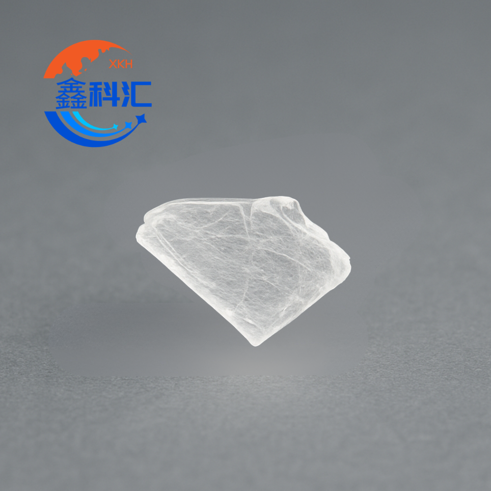
Proč zařízení s vysoce mobilním grafenem závisí na monokrystalech hBN

Graphene is widely regarded as one of the most remarkable materials ever discovered. Its exceptional electrical conductivity, mechanical strength, and atomic thickness have opened new possibilities in nanoelectronics, sensing, and quantum technologies. However, one of the most important discoveries in graphene research is that its performance is not solely determined by graphene itself—but critically depends

Proč zařízení s vysoce mobilním grafenem závisí na monokrystalech hBN Číst více »

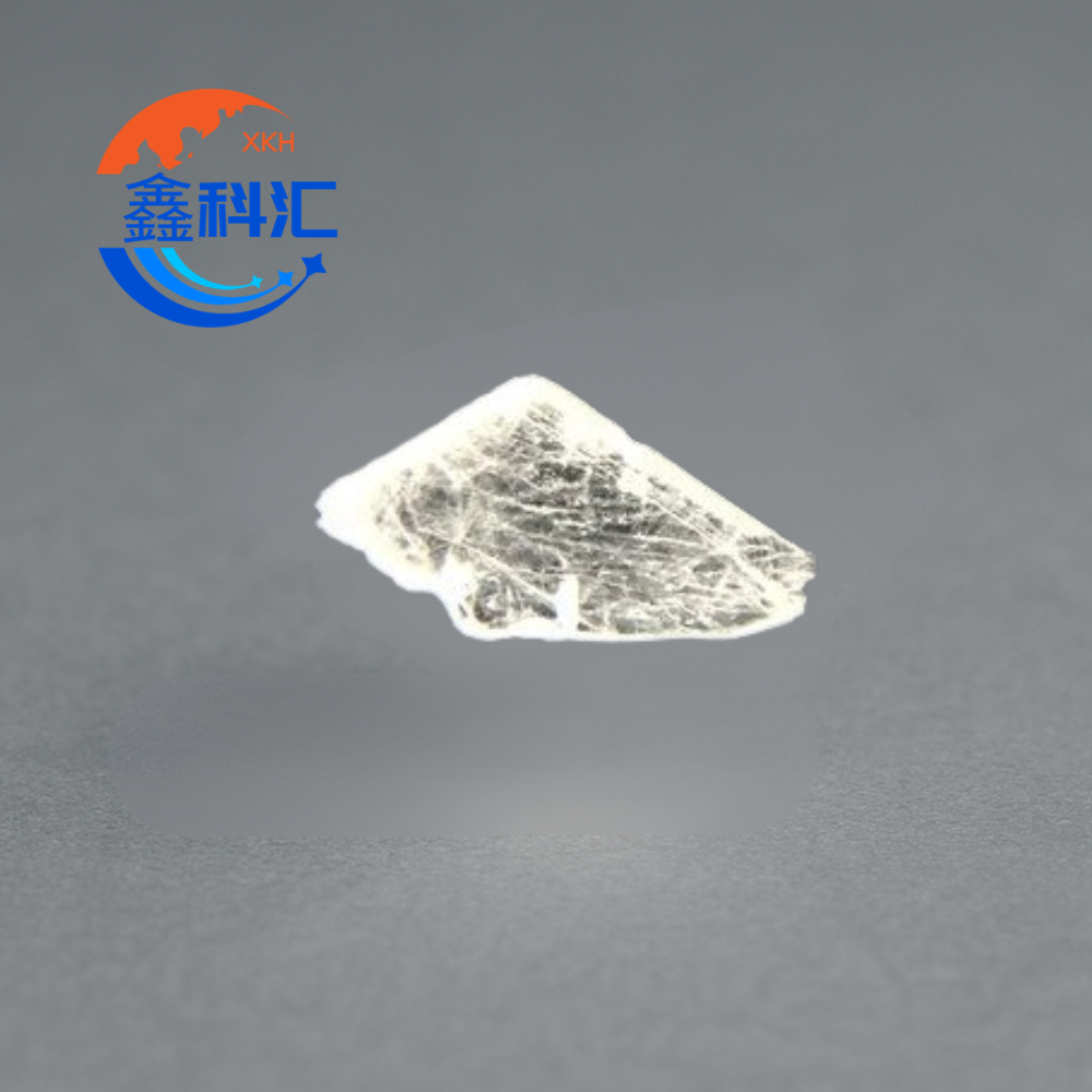
Co je to monokrystal hBN v kvalitě pro elektronická zařízení a proč je důležitý pro pokročilou elektroniku?

As the fields of two-dimensional (2D) materials, quantum devices, and next-generation semiconductors continue to evolve, one material has emerged as a critical foundation for many of the most promising technological breakthroughs: Device-Grade Hexagonal Boron Nitride (hBN) Single Crystal. Often referred to as the “ideal companion” to graphene, high-quality hBN has become indispensable in the fabrication

Co je to monokrystal hBN v kvalitě pro elektronická zařízení a proč je důležitý pro pokročilou elektroniku? Číst více »

Polovodičová keramika: Pokročilé materiály pohánějící moderní elektroniku

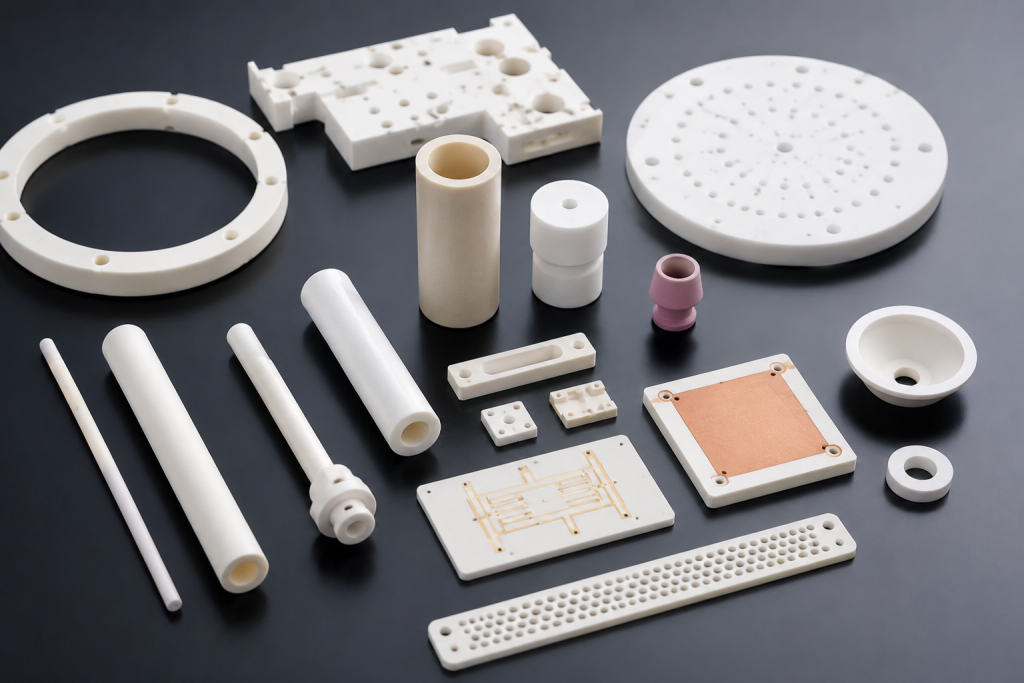
As semiconductor devices continue to become smaller, faster, and more powerful, the materials used in semiconductor manufacturing equipment must meet increasingly demanding performance requirements. Traditional metals and polymers often struggle to withstand extreme temperatures, corrosive chemicals, plasma environments, and ultra-clean processing conditions. This is where semiconductor ceramics play a critical role. Advanced ceramic materials combine

Polovodičová keramika: Pokročilé materiály pohánějící moderní elektroniku Číst více »

Proč je keramika z karbidu křemíku mimořádně odolná proti opotřebení a korozi?

Advanced ceramic materials have become increasingly important in industries that demand exceptional durability, chemical stability, and long service life. Among these materials, silicon carbide (SiC) ceramics have gained widespread recognition for their outstanding wear resistance and corrosion resistance. As a result, silicon carbide components are widely used in semiconductor manufacturing, chemical processing, energy production, mining,

Proč je keramika z karbidu křemíku mimořádně odolná proti opotřebení a korozi? Číst více »

Proces výroby polovodičových keramických součástek: Od surového prášku k přesným součástkám

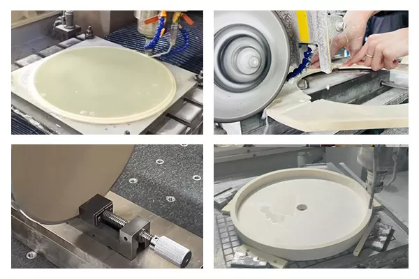
Modern semiconductor manufacturing relies heavily on advanced equipment such as etching systems, lithography machines, ion implantation tools, and deposition equipment. Inside these systems, numerous ceramic components play critical roles in ensuring process stability, precision, and reliability. Thanks to their exceptional high-temperature resistance, corrosion resistance, mechanical strength, dimensional stability, and electrical properties, advanced ceramic components are

Proces výroby polovodičových keramických součástek: Od surového prášku k přesným součástkám Číst více »

Díly z oxidu zirkoničitého vysoké čistoty pro přesné průmyslové aplikace

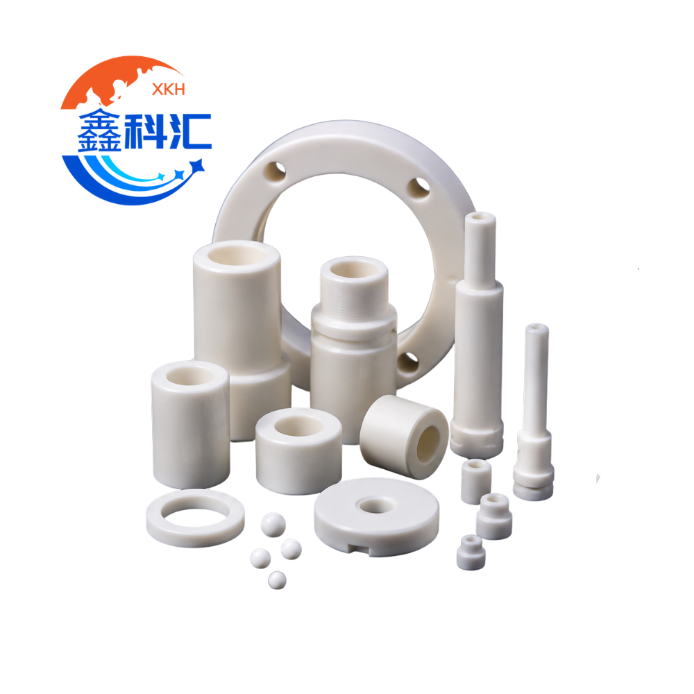
High purity zirconia parts are widely used in industries that demand exceptional wear resistance, corrosion resistance, dimensional stability, and mechanical strength. Compared with traditional metal materials and standard industrial ceramics, zirconia ceramics offer a unique combination of toughness and precision, making them suitable for advanced industrial systems. Today, high purity zirconia components are commonly found

Díly z oxidu zirkoničitého vysoké čistoty pro přesné průmyslové aplikace Číst více »

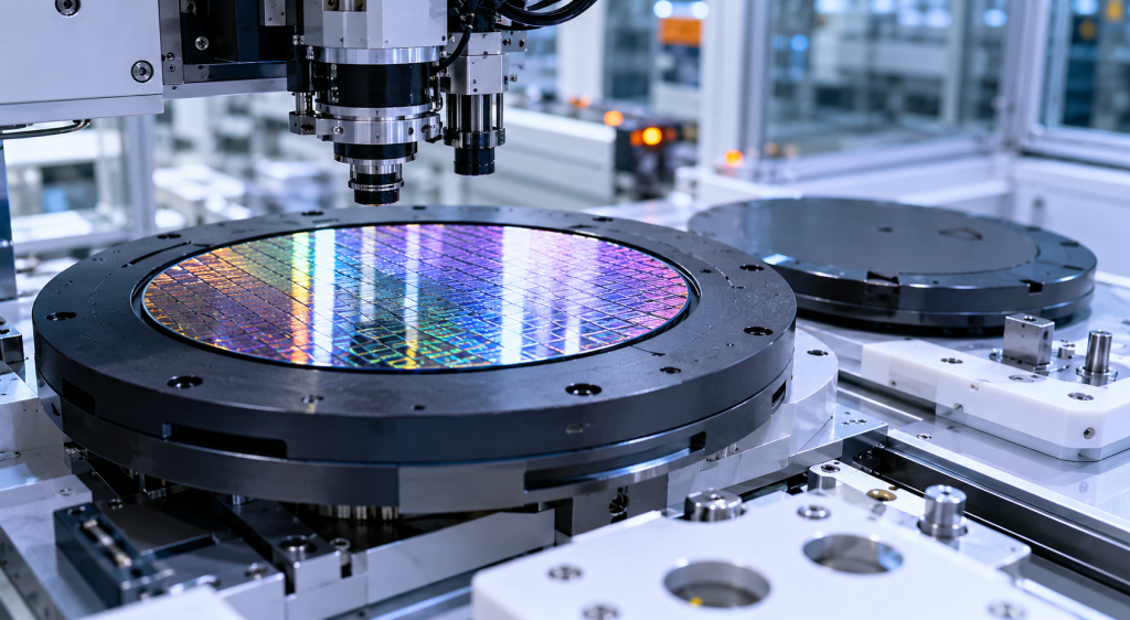
Elektrostatické sklíčidlo vs. vakuové sklíčidlo: Která technologie držení destiček je lepší pro výrobu polovodičů?

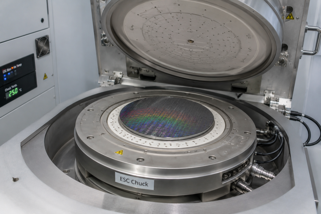
In semiconductor manufacturing, wafer positioning and fixation are fundamental requirements for achieving process precision and yield stability. During etching, deposition, lithography, inspection, and plasma processing, silicon wafers must remain securely held while maintaining minimal contamination and excellent thermal uniformity. As device structures continue shrinking and wafer sizes continue increasing, traditional holding methods face growing challenges.

Elektrostatické sklíčidlo vs. vakuové sklíčidlo: Která technologie držení destiček je lepší pro výrobu polovodičů? Číst více »

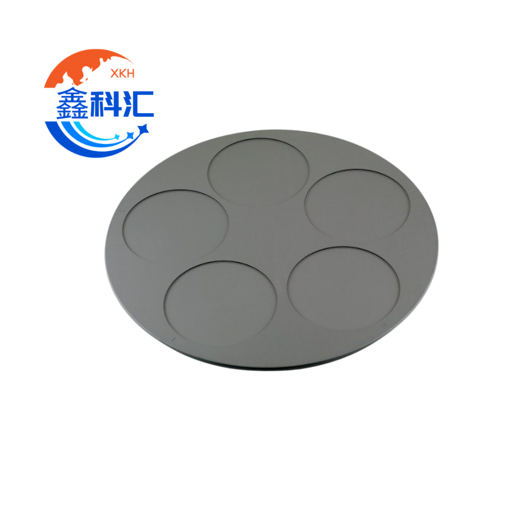
Proč zásobníky z karbidu křemíku nahrazují tradiční nosiče destiček

As semiconductor manufacturing continues moving toward larger wafer sizes, higher process temperatures, and stricter contamination standards, conventional wafer carrier materials are increasingly reaching their performance limits. Components that once met process requirements are now facing challenges involving thermal deformation, particle generation, and shorter service life. Among advanced ceramic materials, silicon carbide (SiC) trays have emerged

Proč zásobníky z karbidu křemíku nahrazují tradiční nosiče destiček Číst více »

Keramický chladič vs. keramický rozptylovač tepla: Hlavní rozdíly a technické role

In high-power electronics, semiconductor packaging, LED systems, and RF devices, thermal management is one of the most critical factors affecting performance and reliability. As power density continues to increase, two terms are frequently used: Ceramic Heatsink and Ceramic Heat Spreader. Although they sound similar, they serve very different roles in a thermal system. In simple

Keramický chladič vs. keramický rozptylovač tepla: Hlavní rozdíly a technické role Číst více »

Od litografie k výrobě destiček: Jak keramika z karbidu křemíku pohání miliardový trh s polovodiči?

When people think about the semiconductor industry, they usually focus on chips, wafers, or advanced process nodes. However, behind every semiconductor breakthrough lies a less visible but equally critical foundation: advanced materials. As semiconductor manufacturing continues to pursue higher precision, smaller geometries, and faster production speeds, equipment performance requirements are becoming increasingly demanding. This shift

Od litografie k výrobě destiček: Jak keramika z karbidu křemíku pohání miliardový trh s polovodiči? Číst více »

Proč je pokročilá keramika v elektronice důležitá? Vlastnosti, aplikace a přínosy

The electronics industry is evolving toward higher power density, smaller device sizes, and more demanding operating environments. From semiconductor fabrication to power electronics and precision sensors, materials are expected to deliver stability under heat, prevent electrical interference, and maintain dimensional accuracy over long service periods. This is where advanced ceramics play a critical role. Materials

Proč je pokročilá keramika v elektronice důležitá? Vlastnosti, aplikace a přínosy Číst více »